• Hello MLAers! We've re-enabled auto-approval for accounts. If you are still waiting on account approval, please check this thread for more information.

PPC750GX vs. PPC750GL?

very interesting! I will have to dig out one of my Factory G3 Uninorth macs (one of my snow iBook's) and see how good or bad its main memory performance is, it will probably be my 750FX iBook G3 since thats the closest I have to your 750GX Sawtooth setup

I would love to see one of your 750GX interposers tried on a 3.3V machine, something like a 1.1Ghz Bondi blue iMac G3 would be quite fun, and in keeping with the "iMac G3" name :)

also of course a BGA225 interposer would be good for as you say upgrading 604 and 603e/603ev based macs

another interposer that I have often talked about with others about hoping to see some day is a 750CXe to 750GX or 7447/7448, since those 750CXe macs have no real upgrade path otherwise
 
I poked around some and it looks like the 750G will easily route to the pads of the 255 pin format of the 740, however there may be some discrepancies. I don't have any machines that use these chips but in this thread stynx shared some pictures of CPU boards with 604 chips removed, and I don't see any unused pads. The IBM datasheet for the 740 shows multiple. I found this picture of a board that can accept a 740 and there are a slew of unused pins (it must use the 32-ibt mode).

68kmla.org/bb/index.php?threads/cpu-swap-ppc604e.48203/
255pads.jpg

Has anyone put a 740 onto one of these boards?

An adapter for the 750CX might be pretty easy, though I have not looked at the pinout. I don't have any of these machines either, so reverse engineering and testing would be difficult.
 
thats pretty sweet! here is a schematic for a PowerMac 6500 Logicboard
I've recently come across the 6500 schematics, which I have been studying a bit for modification purposes

this system uses a CBGA255 603ev, and is compatible with a 740 in that if you BGA swap one on there, it will work OOB (with the only adjustments needed being vCore if your installing a PPC740L or MPC740P)

so perhaps that will give you some clues as to whats going with the pads? :)
 
Has anyone put a 740 onto one of these boards?

Coincidentally, I just fitted a Performa 6500 board with a Motorola 740ARX266, still need to tinker with the PLL, but yes, it does work :)

reballing.jpg

reballed.jpg

fitted.jpg

gaugepro.jpg
 
Hey Daniael,
hows the performance without L2 cache? Does it work with the cache stick? Compared to a standard 6500 with the same speed is there noticeable difference?
also, how to set speed of the CPU (could be useful to overclock a bit the stock board)?
 
Hey Daniael,
hows the performance without L2 cache? Does it work with the cache stick? Compared to a standard 6500 with the same speed is there noticeable difference?
also, how to set speed of the CPU (could be useful to overclock a bit the stock board)?

So, ooof. A G3 without a cache takes a mighty oomf to its performance. I know the L2-less Wallstreets were pretty bad
 
@Powerbase, yeah! I had even replied to that, really really fascinating. I wish I had a larger preheater than the 853A, I'd love to try this....
it seems from re reading that thread that it is indeed possible to use the L2 cache that the 603e came with on the board, and that it does some good...
 
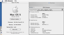
The CPU clock speed is not reported correctly and I would guess that another PVR check is used there, which also reads HID1 to calculate the CPU speed and populate the device tree
Just been thinking about this, which PLL are you using/setting to achive 800Mhz? since I know the 750FX and 750GX are a bit sepcial in that they have 2 PLL's PLL0 and PLL1, so I wonder almost if the Sawtooth BootROM is reading from the wrong PLL range?


also as an aside if the 750GX supports 32 bit bus operation, does that mean that one could in theory make an interposer and fit one to a Power Macintosh 5200? :) it would be bottle necked to buggery, but it would be fun to push such an infamous system to its utter limits :) (I think those systems use QFP CPU's)
 
I believe there is a PVR check that doesn't recognize the 750G, so it apparently defaults to some generic PPC 60x. At 800MHz (100MHz bus x 8) the PLL_CFG for 8x on the 750G is 10000 and it reports 300MHz, which agrees with the setting for 60x 1000. At 1.1GHz the 750G setting is 10101 and it reports 400MHz, where 60x is 1010. That's not conclusive but I think I see a pattern...

The nice on-chip L2 cache should help a lot on bus constrained systems. Also, the bus multiples go up to 20x so you could have a 1GHz G3 on a 50MHz bus.
 
I believe there is a PVR check that doesn't recognize the 750G, so it apparently defaults to some generic PPC 60x. At 800MHz (100MHz bus x 8) the PLL_CFG for 8x on the 750G is 10000 and it reports 300MHz, which agrees with the setting for 60x 1000. At 1.1GHz the 750G setting is 10101 and it reports 400MHz, where 60x is 1010. That's not conclusive but I think I see a pattern...

interesting sounds like its not recognising the last PLL bit properly, If I recall correctly of the patches offered in the Powerlogix Patcher is for to patch the system for correct PLL/frequency reporting, I take it you you have tried selecting that option? (but maybe out of the box its only patching for 7447/7447A/7448's and needs further patching for 750GX?)

I know its just a cosmetic thing, but im an "About this Mac" Junky, so would be sweet to see the "1Ghz G3" in all this glory

BTW one fun thing to do with one of your G3 cards and sawtooth or an MDD, is install 2GB of RAM, until now theres never been a system with a G3 that could take more then 1.5GB :)


BTW going back to your earlier test with the PPC750S CPU, was there any resistors/straps you had to change on the AGP CPU card, or where you able to just solder it in place of the previously removed G4 CPU? I have a number of PPC750S/PPC750L CPU's I have pulled from various systems I have G4 upgraded over the years (mainly Pismo's, but also a Clamshell iBook G3 and a slot loading iMac G3 :) ) so I would like to try installing one onto a G4 CPU card


The nice on-chip L2 cache should help a lot on bus constrained systems. Also, the bus multiples go up to 20x so you could have a 1GHz G3 on a 50MHz bus.
yeah thats exactly why I was mentioning it :) In that regard with your 750/7400 to 750GX interposer it would be fun to try one in a PowerBook G3 Kanga, another Orphaned mac, its pretty much a PowerBook 3400c with a G3 750 and backside L2 cache slapped onto it, and unlike every other G3 system from apple, its based on a pre-gossamer platform, its PSX+ and O'Hare, as such its also the only G3 system that apple never officially supported with Mac OS X or Mac OS 9.2.2 (although xpostfacto and OS9Helper works around that :) )

a G4 7400 on a Kanga is another I would love to see someone try some day, just because then in theory it would be possible to run Leopard on one, imagine that! :)


as an aside does anyone have a picture of one of the 750FX/750GX PowerLogix CPU card for the PowerMac 7300-9600 machines? I have seen a few ZIF ones for G3 beige/G3 Blue and white etc, but I dont think I have actually seen any detailed pictures of one of the 7300-9600 750FX/750GX cards, I wonder if it would be possible to remanufacture those also
 
but does beg the question what does the 750GX in those PowerSurge OWR systems show up as, when *not* running any 3rd party extensions/software/utilities, IE if you boot a stock install of Mac OS 9.1 and use a stand alone utility like Gauge Pro or Metronome to query it? or go into OpenFirmware do a .properties on the cpu itself in the device tree that would be quite interesting to see in its own right :)

the reason I mention the G3 beige is because of how it did see the CPU as a regular G3 rather then displaying it as PowerPC 60? with the 750GX PVR as I would have expected it to do (like for example what it does with a G4 CPU, obviously displaying the G4's PVR in those cases)

PS do you have any pictures of those cards? I dont think I have ever actually seen one pictured, I have only read about them from period articles and on the old XpostFacto Forum, so it would be cool to see what one actually looks like after all this time

I did a bit of digging on this front, turns out OWC themselves still have a couple pictures of the card on their website still, including one with the heatsink removed


plgpcigx10001largenohs.jpg
check out that bodge wire on the top right in the power-supply section :)


but along with these one thing I have been wondering, is what sort of level shifters are avliable these days? as I understand it the 7300-9600's systems work with a 5V logic level, so even a standard G3 750 requires a bunch of level shifters to work in those systems, which is what I think the IC's going acrosss the slot is there for

but it makes me wonder if your already doing logic level shifting, are there logic-shifters that can go from 5V right down to 1.8V? because then that would allow you to use a 7448 with such a system, which would be really quite awesome, I know sonnet must of figured something out since they did make a 7450-7455 based for the 7300-9600

 
Been doing a bit of internet sleuthing recently mainly to figure out the whole mystery of the PowerBook 1400 and the PowerBook PowerPC upgrade card that you can read about in @Daniël's BGA thread

but while doing that, I did start to wonder just where *did* all the IBM PDF's go? thankfully for motorola designs we still have NXP and they have a nice stash of PDFs still thankfully, but what happened to all of IBM's stuff?

while I dont have a direct answer to that, I did find where they used to be back in the day and thankfully the archive.org has some of the pages/pdfs archived


and one that I noticed which I think is worth posting in this thread, and relevent espically to @max1zzz is this nifty PDF


that details the differences between the 750FX and 750GX :) thankfully I dont see obvious any-show stoppers (apart from the need to patch the iBook BootROM), but figured its a good document to have on hand just incase :)


also of note is this very handy document which goes into soldering these CPU's and their weird BGA balls, including solder-stencil design details


@herd also talks about them here as well :)

Thanks for sharing your experience. The OEM chips typically used a 0.89mm Diameter 90% Pb and 10% Sn (by Weight) “High Melt” solder ball held between CBGA substrate and PCB with regular eutectic (63Sn/37Pb) solder. The idea was to have a ball that would not collapse when attached. The resulting column of metal would allow some flex to accommodate the difference in thermal expansion between the ceramic and PCB. This was later addressed by the HCTE substrate, and these chips could be soldered directly to the PCB with relatively thin fills.

So basically, to attach a 90/10 ball to a copper pad, you need to add some solder. Solder paste is the typical solution, but other methods are possible for hand assembly. It is not really feasible to directly attach the “High Melt” solder ball to the pad because extreme temperatures would be required and if the ball collapses then there would likely be other problems too.

Or you can remove the OEM balls and use smaller/shorter 63/37 balls. The long term thermal fatigue performance will be reduced somewhat, but BGA technology has proven to be more reliable than skeptics feared at its debut.

as an aside learning about the fact that the solder balls on PPC CPU's where not actually solder balls in themselves but more interposer balls, and that they where soldered with regular solder paste, finally not only solved the mystery of just what where those balls, but also solved a mystery that had equally baffled me for a long time and that is, why did some single cpu upgrade cards built on dual CPU PCB's still have solder on the un-used 2nd CPU BGA's pads if there never any CPU there? of course now I know they must of used the same stencil regardless and so it got solder-pasted even tho no CPU was being installed :)

1726023224546.png
 
Last edited:


check out that bodge wire on the top right in the power-supply section :)

I wonder if that bodge wire is there to carry extra current. It can be tough to get enough trace volume to carry good power supply current.

but along with these one thing I have been wondering, is what sort of level shifters are avliable these days?
Not really where you were going with that, but IIRC, those are these which are still available, but EOL. There are probably substitutes available.

https://www.digikey.com/en/products/detail/texas-instruments/SN74CBT16861DGVR/377881
 
I wonder if that bodge wire is there to carry extra current. It can be tough to get enough trace volume to carry good power supply current.


Not really where you were going with that, but IIRC, those are these which are still available, but EOL. There are probably substitutes available.

https://www.digikey.com/en/products/detail/texas-instruments/SN74CBT16861DGVR/377881
interesting :) I figured those where level shifters to shift the 5V level 60x bus from CPU slot to a 3.3V or lower level for the CPU itself
 
Another quick note on the G3 bus speed: I was playing with the AJA System Test software. This is usually for testing hard drive speeds, but if you enable the file system cache it turns into a sort of memory speed test. The G3 speed is less than half of the G4 with everything else unchanged. This result duplicates others noted previously, strange though it is. With the file system cache disabled, there is no difference in hard drive speed. I did not try high speed cards like 64-bit PCI RAID. I think these would be limited by the G3 memory speed.
 
"A G4 CPU is just a G3 with vector instructions tacked on."

I've heard this dismissive phrase many times over the years. Maybe it was coined in response to marketing hype about altivec when the G4 came out? In my experience the G4 was always significantly faster than the G3, even when running software written for the G3. Thinking about this more after playing with the 750G chips and subsequent renewed interest in the G3, I kept trying to figure out why the G3 was slower than expected. After doing various experiments and researching the subject, I've finally come to the conclusion that the phrase above is wrong. It should be, and should have always been:

"A G4 CPU is just a G3 with a 3x faster bus (and vector instructions)."

I eventually found a paper that mostly explains the hardware differences responsible for the results I kept finding. I've attached it below if anyone wants the details. Of course there are a number of small changes between and among the two families of CPUs: things like slightly different cache implementations, more/less cache, better/worse FPU, etc. all of which could amount to a few percent in general or noticeable differences in limited cases. But with altivec aside, the biggest difference is summed up with the revised phrase.

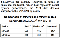
How has 300% not been the main story this whole time?!? Wasn't DDR a big deal? Here is a relevant excerpt:

G3vsG4bus.png

That is comparing the two chips at the same speed with the same 60x bus. The G4 also enabled the MPX (aka maxbus) mode that could further improve speed (~20%). Here are some simple results that include that twist:

68kmla.org/bb/index.php?threads/interest-in-adapting-744x-to-7400.41677/post-536211
 

Attachments

Back
Top