• Hello MLAers! We've re-enabled auto-approval for accounts. If you are still waiting on account approval, please check this thread for more information.

Project30 - fourth edition - Radius IIsi NuBus Adapter build for SE/30?

Trash80toHP_Mini

NIGHT STALKER
68040
Five years and two days to the date, Project30 is back on the bench thanks to new developments.

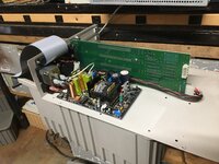
Replace the IIsi NuBus Adapter in this pic from back then . . .

SuperMac-IIsi_NuBus-Cards.1.jpg

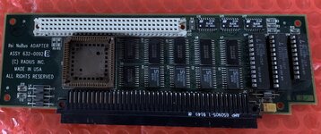
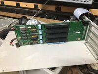
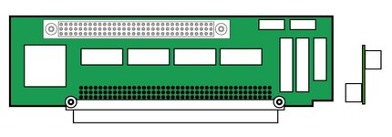
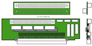
. . . with this card we found at the time . . .

Radius_IIsi_Nubus.jpg

. . . add the 40MHz clock from the former to the Radius adapter and we've got a whole new ballgame for the SE/30.

Multiple NuBus slot possibilities for the SE/30 and IIsi listed here:


@Bolle & company, whatcha thinking? Have you got the schematic to post?
 
Last edited:
Hey Trash,
This is something I've I wondered about for years. CongraduIations to team Project30. I was under the impression that other parts would have to be added to the board. Do you think I can now use an OTTO TECH SEIV with this mod? Peace.

TPOPE
 
Thanks, that was a long way coming, though not there yet by any means. Project30 was the code name for NuBus-in-IIsi I came up with for the first edition thread over at ThinkClassic even longer than five years ago.

SCSI II in an SE/30? Dunno if that would like running at 8MHz on the Radius NuBus adapter as is. Dunno if @Bolle tried that? Other cards seem to have functioned well enough. Hope here is that we can rework the Radius adapter with the 40MHz clock implementation of the other two candidates.

The DuoDock is really my preferred implementation, two slots right out of the box!

TwinSlot-NuBus-Adapter-xi.JPG

I'm hopeful we can use the stock TI Chipset Apple may have relabeled on that fork of the project. I'll have to check the dates on that some day. Transceivers are probably just rebadged TI parts? Dunno about what Apple might have done to further bork the Mac II setup when they transitioned from GAL implementation in first edition II to NuChip in the second release?

Apple played fast and loose with the NuBus standard they helped get off the ground, but there's a slim chance their TI controller run was a rebadge as well? Checking the dates of TI's move from 020 to 030 controller against NuChip to NuChip30 transition might prove interesting?

Hopefully we can wring 2-3 slots out of the very simple Radius adapter on the 20MHz IIsi PDS shared with the Duo's 030 PDS Docking connector that aligns nicely with the IIsi PDS clock. Taking it clock independent for the SE/30 would be the thing here?

Knowing the brand of wizardry practiced by the renegade Mac Developer trio at Radius, it may very well be set up for addressing only a single slot. Whereas Apple just used the stuff they had in the parts bin and schematics to cobble together the IIsi NuBus Adapter on a shoestring.
 
Last edited:
Had another thought about this crazy simple NuBus Adapter. Morning musing WAG of the day:

Might the wizards at Radius have cut the controller out of the schematic entirel? That would set the PDS up to control only a single card from MDU directly through the GALs onto the MUX ICs?

Dunno about ramifications for adding the 40MHz crystal can for clock independence from the 16MHz SE/30 bus in that case? But it works with the pre-MDU SE/30 Memory Controller setup.
 
Last edited:
Might the wizards at Radius have cut the controller out of the schematic entirel? That would set the PDS up to control only a single card from MDU directly through the GALs onto the MUX ICs?
Thinking about it more, I'm not sure there's anything to gain in the 'controller' by assuming there's just one slot. In fact, I think the 'controller' is pretty much just a NuBus master/slave device - the master side propagates the requests from the CPU bus, while the slave side takes request from the other masters and translate them into CPU bus request.

Not an expert here (I hadn't looked at the NuBus specifications before the last end-of-year vacations...), but to go from 1 to N slot, you only need:
a) to add a /NMRQ line per extra slot going to the interrupt handler - that goes to the VIA2 and not the NuBus logic so shouldn't affect the 'controller'
b) to add the proper pull-down on the /ID* lines so each extra slot can identify itself - again the 'controller' doesn't care;
c) the arbitration logic is shared lines between masters - again the 'controller' doesn't care how many other masters there is (except for extra contention), if it has to compete, competing with 1 or N other master(s) is handled the same way.

The four FSM of the 'controller' described in the DCDMIIMSE (1-8) don't seem to care, either.
a) one is just the time-out to generate an ACK to /START when no-else does - that's probably the only thing special about the 'controller' compared to other masters on the bus;
b) bus-to-nubus (master) only look at addresses; presumably anything in the NuBus areas is transmitted - one could avoids some time-outs by rejecting addresses for non-existent slots, but it would be extra logic for not much gain (and any such filtering would probably be identifiable from a schematic + PLA logic);
c) nubus-to-processor-bus (slave) "controls accesses from the NuBus, through the processor bus, to RAM, ROM, and I/O." It is only concerned by the destination, the source is just "the bus" - whichever master on the bus doesn't seem to matter (and shouldn't per the specs);
d) NuBus slave state "tracks the state changes on the NuBus" synchronously - AFAICT there's no information on the bus itself about how many devices there is or which one is currently active; the arbitration is between masters as mentioned previously; the slaves only look at the addresses to decide whether to answer or not; this is just the 'normal' bus tracking in all likelihood.

So I don't see anything one might cut off from the 'controller' (which is just those state machines implemented in one chip, I suppose) and still have a proper NuBus implementation.
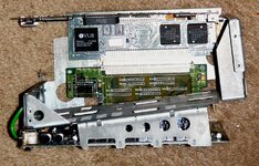
 
Interesting! We've three(?) reserved lines on the 030 PDS available to the new build logic boards. You might consider options for implementing those in the proposed multifunction adapter riser with NuBus?
 
We'd talked about schematic development of NuBus in Macintosh II v.1.0 and a member just happens to be in the process of troubleshooting that very board. Detailed pics there. Direct link to overview pic: Thought here is to strip away the NuChip implementation from the existing Mac II schematic, place components in a visual diagram and buzz connections in order to begin to get a picture of what's going on there?

Found something new and very interesting on the DuoDock NuBus front as well. Still trying to determine version dates and align them with the two relevant Block Diagrams in order to wrap my head around it. Might be promising? Dunno, but it's definitely yet another window into Apple's implementation of the elusive NuBus critter. :)
 
Last edited:
Here are the three "Reserved" pins on the 030 PDS and everything else but Address/Data buses. ISTR a reserved pin in one machine/adapter or another having been connected to something, but damfino what it was at this point. Pin 2C lost its /NUBUS or n.c. label below.
IIsi-S330-PDS-01.JPG
If the reserved lines don't go anywhere on IIsi or SE/30 logic boards that'd be ideal. If they do go somewhere, maybe they can be cut without borking anything? In either case they might be patched to wherever they need to go on either machine's logic board to run necessary lines up the riser to implement more than a single slot?

Column labels went missing too! Top's A, bottom's C.
 
Found something new and very interesting on the DuoDock NuBus front as well. Still trying to determine version dates and align them with the two relevant Block Diagrams in order to wrap my head around it. Might be promising? Dunno, but it's definitely yet another window into Apple's implementation of the elusive NuBus critter.
Well, it looks like that a window into implementing the elusive NuBus in DuoDock on 030 PDS may be closed, but who knows? Maybe it's ready to unlock, but the storm window is in place or hopefully only the screen will remain in the way?
________________________________________________________________________________________________

Duo System DevNote:

NuBus Controller 14

The NuChip 34 controls the interface with the optional NuBus cards. It is similar to the
NuChip 30, but with modifications that enable it to run at 33 MHz.
NuBus cards occupy slot and super-slot segments C and D of the PowerBook Duo
computer’s I/O space. (The flat panel video display occupies the address space normally
occupied by NuBus slot 6. External expansion video and most I/O appear in the address
space normally occupied by NuBus slot E.) Table 14-11 shows the I/O space for the
NuBus cards.

Table 14-11 NuBus I/O space
Starting address Ending address Comments
FA00 0000 FDFF FFFF NuBus slot space
A000 0000 DFFF FFFF Super slot space
________________________________________________________________________________________________

What's most interesting is what Apple meant by "NuBus slot 6" in that diagram? I'm thinking $E because the LCD becomes inactive when Docked and DuoDock video is located at $E with the rest of the Dock's functions.

The one hope remaining for the DuoDock fork in development would be those very curious NuChip 30-33 and NuChip 34 characters in DuoDock, DuoDocks II and the later Duodock+ pared down to minimal spec***** for the 2300c. Has anyone seen either in the block diagram of any other Macintosh?

If not and they really are unique to the PowerBook Duo System that could be very interesting indeed. 😬 Back down the badger hole.

***** https://apple-history.com/duodockii
 
Last edited:
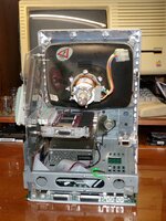
Pic links in the other threads seem to open up random uploads now? So here are a couple fitment config test pics.

8vRuFk.jpg

ErGvUC.jpg

Project30-Testbed-03-1p.jpg

It'd be nice to get a pair of slots up and running in the SE/30 a/o the SE/30 form factor scrunched IIsi/ci board, but just one may have to do. I'd be happy just getting that Little Red Radius Pixel Rocket into my SE/30.

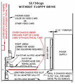
Used a pair of NICs atop a Zip stand in for the HDD, but the Gamba "slap the HDD upside the PSU side config" opens up all kinds of cubic for expansion card playtime.

030cgs_stack_wo_floppy.gif
Obviously, the proposed multifunction riser won't need interfere with the FDD in either Logic Board configuration.
 
Hi, I messed with trying to get a Nubus adaptor to work in a SE/30 about 15 years ago.
I didn't do much, just plug a Nubus adaptor into a SE/30, You know rth results.
But I did get this.

Attachments​

  • IMG_0312.JPG
    IMG_0312.JPG
    2.1 MB · Views: 12
  • IMG_0311.JPG
    IMG_0311.JPG
    2.2 MB · Views: 13
  • IMG_0313.JPG
    IMG_0313.JPG
    2.4 MB · Views: 13
  • IMG_0314.JPG
    IMG_0314.JPG
    2.3 MB · Views: 14
  • IMG_0315.JPG
I didn't get the board that goes in the SE/30.
johnsn

I posted this on the rev 3 of this thread.
 
(...)the Radius adapter(...)
Has anyone seen one of those? Do they have chips on the back or just the front? Looking at it again (prompted by this thread), it only has six 8-bits transceiver chips instead of the expected eight. There's also more ALS240 than in Apple's implementation, so maybe a slightly different bus driving scheme. If those GAL/PAL can be read for configuration, all the chips are still being made, that one would probably the easiest of all implementations to replicate.
 
GALs from the Radius adapter have already been read long ago:

Downside with the Radius adapter is that it will run synchronously at half of the host clock… in a IIsi that works out perfectly to run a 10MHz Nubus clock, in the SE/30 that design will run Nubus at 8MHz.
The state machine they implemented doesn’t account for asynchronous operation.
 
GALs from the Radius adapter have already been read long ago:
Neat. Did anyone trace the board as well?

Downside with the Radius adapter is that it will run synchronously at half of the host clock… in a IIsi that works out perfectly to run a 10MHz Nubus clock, in the SE/30 that design will run Nubus at 8MHz.The state machine they implemented doesn’t account for asynchronous operation.
If it is running half-clock just to avoid the cost of an extra clock, then it's an easy fix. If it's somehow requiring the clock to have some relationships in the GAL/PAL, then it will be harder to 'fix'. But in either case, with the appropriate schematics, it should be possible to recreate the board with either modern PAL/GAL or replacing them all by a single CPLD, and then figure out how to 'improve' it.

As for synchronous, that's for slave mode I assume, as for bus mastering they have little choice, I believe the IIsi memory controller is fully synchronous and will only answer with /STERM.
 
Pretty sure it’s about more than just adding a clock oscillator.
The implementation is so simple because it doesn’t have to glue together two different clock domains of the Nubus and processor bus.
Apples discrete Nubus implementation needed 12 PALs instead to do this, so I don’t think it’s easily added to the simpler Radius one.

I reverse engineered the Mac II PALs as well btw:
 
Pretty sure it’s about more than just adding a clock oscillator.
The implementation is so simple because it doesn’t have to glue together two different clock domains of the Nubus and processor bus.
Apples discrete Nubus implementation needed 12 PALs instead to do this, so I don’t think it’s easily added to the simpler Radius one.
Indeed, you can generate the required 10 MHz 75% duty cycle of NuBus by just 'masking in' every other low pulse of the 20 MHz 50% duty cycle CPU clock, giving you a fixed phase relationship between the two. If Radius exploited that (and it seems likely they did), then I agree it would be much more difficult to leverage to an arbitrary CPU clock. Still an interesting implementation to study, IMHO, as it probably can't get any simpler than that.

I reverse engineered the Mac II PALs as well btw:
Another bit of good news! Thanks for all those efforts.

Unfortunately, it seems the only available schematics for the Macintosh II (from bomarc) are for the later version using the NuChip. So, as for the Radius adapter, without some idea of the schematics (in schematics or at least traced PCB) connecting the PAL/GAL and buses, it still requires a *lot* of reverse engineering :-(
 
Funny that this thread should pop now! Had another crazy notion that much simplified a project that's been on the back burner for quite some time. Been trying to adapt the Radius adapter in its native IIsi environment while providing for a PDS connector underneath as well.

Looking at it again (prompted by this thread), it only has six 8-bits transceiver chips instead of the expected eight.
The DuoDock+ employs a quartet of skinny little ACT16651 16bit transceivers. Placing a 1x4 row of these clears up enough PCB real estate to put an interboard connector for a PDS slot daughtercard with connector in the position of the lower slot of my TwinSlot PDS riser for the IIsi.

- Putting the thruhole PDS Connector on the main board is impossible
- The big square transceivers of the Apple adapter won't fit between NuBus and interconnect for daughtercard

Knocked together this rough of the plan last night and this morning.:
NuBus-PDSrough.jpg
"Periscope" PDS daughtercard is on the right. Original plan was to harvest Apple's NuBus Controller and stick the FPU socket in the space of the Radius controller on the right side above. Has anyone done a schematic of the Apple adapter?

New parts available Radius adapter is the new goal. Cannibalization of the Apple controller is then avoided for all but my one off prototyping effort.

@Bolle does the periscope PDS adapter board provide enough real estate to work your magic in four layers?
 
Figured out why that first rough in of the plan didn't look right this morning. The Passthru connector was overlaping the motherboard connector pins OOPSIE! No wonder there looked to be far too much room between interconnect and NuBus slot.:oops:

I'm figuring that just about any expansion card in the PDS Slot will have a socket for the FPU. So that's been eliminated in hopes of doing this version of the Radius NuBus adapter in just four layers?
Connectors-n-Bits-02.jpg
Thinking a straight thru path from PDS->Buffers->Transceivers->NuBus Slot will be optimal in its simplicity? Gray chips are the buffer/line drivers on the solder side of the PCB. There are a few more bits to add to the layout, but thinking I've got the major components configured into what might be possible in four layers?

Dunno, whatcha think gang?


p.s. since it's my Project30 topic, I'll forgive myself for sending this tangent back into the IIsi realm. I'll start a topic where I can look at drawings full size and print them out at work.
 
Last edited:
Those ACT16651 are apparently still current, but Mouser doesn't stock them, they're not cheap, and MOQ is 80. '651 or '648 are probably a cheaper option.

For cost reason, you really want all your SMD components on one side if someone like JLCPCB is to assemble them.

I would recommend first doing a prototype without too much worry about fitting in a case, just to make sure the interface can be made to work (and potentially expanded to more than one slot).

Beware of the data order from PDS to NuBus; first NuBus is multiplexed so all 8 drivers are going to NuBus A/D signals while half of them will go to the PDS D ,and half to the PDS A. And the byte order for D is reversed as NuBus is little endian. And having done some tests at one point, IIRC, the byte/bit order is the opposite between NuBus and PDS... The routing is not simple.

@Bolle Beyond the clock, maye Radius has cut some corners with the arbitration as well (for bus mastering)? With just one slot at a known address, you probably don't need to look at all ARB signals...
 
Back
Top