• Hello MLAers! We've re-enabled auto-approval for accounts. If you are still waiting on account approval, please check this thread for more information.

PPC740L G3 CPU Daughterboard For Blackbird Powerbooks

Damn, looks like it's 32 bit. Found the spec in the PowerBook 550c ServiceSource introduction.
Yep, and it's the same for the Service Source for the rest of the BlackBirds, Series 500 Service Source,. Well, that's a Hard Stop IMO. There is no reason to expect the 603ev to operate in 64-bit mode when the data bus was 32-bit and it could operate in 32-bit mode. The Pratt wouldn't be designed to handle 64-bit data bus translation when the only Apple approved upgrade could operate in 32-bit mode.

It looks like those rumors about the guy in Japan that transplanted a G3 were indeed just a rumor, since it is literally not possible.

Okay, well, I consider that a wrap. Thank you all for helping with this, your input has been invaluable, but, unfortunately, we have hit an insurmountable problem. I'm glad this was found before CC's daughterboard was sacrificed in vain.

Unless someone can provide hard evidence that this isn't a problem, I'll consider this project terminated.

 
The only hope now is to use a 745, since it can run in 32-bit mode, but the B01 pin issue needs to be rectified, and, of course, the core voltage would have to be adapted to handle a processor with a 2.0 V core. Both issues are way beyond the scope of this thread. So, if anyone wants to pursue adapting the 745 to the BlackBird PowerPC upgrade daughterboard, please start a new thread, since this one should be considered finished, unless someone can think of a way to adapt a processor that expects a 64-bit data bus to a system with a 32-bit data bus

 
Your project isn't finished, it just got far more complicated! [:)] A new processor card designed around pads for the 745 addresses every problem I can think of offhand. Unlike my theoretical 1400 processor card design, you have the added complication of harvesting Apple ASICs, ROM and misc. components to utilize on your board, but that's not insurmountable. You have but a single interboard connector, where I need to align two of them perfectly as required in a 1400 processor card.

BTW, what the blazes is that is that very long, very high pincount white connector on the floor at the front of the processor card cage? Can't figure it out from the block or exploded diagrams. The cubic is occupied by the Modem Card in the exploded diagram, but that's an insanely high pincount for a simple modem interface. Who needs a modem for a PowerBook in this cord cut cellular era anyway? Any clues as to what Apple might have had planned for that crazycool connector would be much appreciated.

Good news is that you've got the cubic to use a a 10cm long board with integrated MaxRAM. Without the memory card's board interconnect blocking the way, you can use something like a full size 7cmx10cm copper heat spreader. to keep your cooling budget in line. Added benefit of leaving out the Modem would allow cooling fins to be soldered to the bottom of my proposed copper heat spreader in its place.

Such would be a fab subject of another thread for you to explore, even theoretically. [;)]

 
Last edited by a moderator:
Yeah, that honking white connector is for the modem, hard to imagine they need one that size. That sucker is 100 pins. They used 64 of them just for address and data bus. Insane design.

Hard to believe there weren't more PDS cards for the BlackBird. It's a typical PDS interface, just like any other Mac.

A far as the 745, I'll have to leave that to someone else, once it rises to the level of using an interposer or a whole new card, I have to bow out.

 
Last edited by a moderator:
Yeah, that honking white connector is for the modem, hard to imagine they need one that size. That sucker is 100 pins. They used 64 of them just for address and data bus. Insane design.
Is there documentation on the BlackBird Board Interconnect pinout? I need documentation for the 1400 system interconnect as well if someone tries to dig that up. Maybe Inside Macintosh has them?

Hard to believe there weren't more PDS cards for the BlackBird. It's a typical PDS interface, just like any other Mac.
PDS Cards were only 16bit as would supposedly be the rest of the I/O bus according to the DevNote block diagram, which appears to be in error.

View attachment 25852

Pinout for the PDS has all 32 Address/Data bits, so 16bit system bus may be a typo. But I'm beginning to think it might be a red herring? Again, is there documentation on the System Interconnect pinout anywhere? Is it 16bit or 32 bit? Pincount suggests 16bit to me, so that insanely great Modem Connector (documented!) is beginning to look like a full blown 32bit PDS/Alternate System Interconnect to me because the pinout appears to have all the control lines necessary for a PDS. 

I know I'm bat shit crazy, but this might actually not be such a crazy notion at all? :huh:

 
Here is the pinout for the modem connector in the Developer Note for the BlackBird series:

http://mirror.informatimago.com/next/developer.apple.com/documentation/Hardware/Developer_Notes/Macintosh_CPUs-68K_Portable/PB_520_520c_540_540c.pdf

Here is the Developer Note for the 1400:

http://mirror.informatimago.com/next/developer.apple.com/documentation/Hardware/Developer_Notes/Macintosh_CPUs-PPC_Portable/PowerBook_1400.pdf

I would imagine it has the pinouts for anything you would be interested in

 
That's what I've been working from. I've never seen any Apple documentation on a Processor Card interface. That would likely have been a deliberate roadblock for third party accelerator development. After all, Apple wanted us to by newer/better/faster Macs/Books. Extending the useful life of one we'd already bought with a third party upgrade made/makes no sense at all from Apple's perspective..

Just dragged a screwdriver across the System Interconnect bumpage and came up with something like 80 pins. The images in the back of my head suggest that the Modem Connector is almost certainly capable of supporting a full length Processor card in that conveniently long RFI corral. I also see a subterranean 32bit bus between PDS and Modem Connector. Buzzing the three connectors ought to tell that tale, the Modem Connector is almost certainly the place to put a new Processor Card design if my hunches are correct. G4 anyone? :lol:

 
I noticed that as well when looking at the Developer Note, no processor daughterboard pinout. I figured that was deliberate. Damn Apple!

I figured the 3rd party guys probably just grab a system and reverse the pinout themselves using the brute force method.

 
I figured the 3rd party guys probably just grab a system and reverse the pinout themselves using the brute force method.
Ayup, gotta do just that for the 1400 connectors, what a massive PITA!

DRAT! I've got shrink wrapped docs/disk for the  Global Village PowerPort/Mercury in the BlackBird parts bin and no Modem in sight. No BlackBirds, don't really want one, but  .  .  .

Best/easiest way to test my theory would probably be to harvest a connector for the Modem Slot from a Modem and one for the System Interconnect from a logic board. Brute force the System Interconnect pinout and design and send Gerbers off for a System Interconnect to Modem Connector adapter and see if a 68040 card fires up in that config.

So far as the dearth PDS cards go, that may have been a direct result of the 16bit/32bit disparity. Anything for the PDS hobbled to 16bit would have made it a PCMCIA card candidate?

edit: just realized ti wouldn't be all that bad to brute force the System Interconnect pinout.  Hold one probe on one of its SMT bumps and drag the other across those of the documented Modem Connector. The missing signals will be the high order data bits and any control signals that don't need to make the trek down to the logic board, but will need to for a full PDS implementation.

 
Last edited by a moderator:
Well, it turns out this project may not be as dead as I thought. It turns out that the memory controller and bus translator IC that NewerTech used for the NuPowr 167 was a later version of the one that is typically used in the BlackBird series and is capable of translating the 64-bit data bus that the processor uses "into single or multiple MC68030 dynamically sized bus cycles. Because the IC seamlessly integrates the two buses, the microprocessor and other bus masters operate as though they were on the same bus." This is from the BlackBird developer note.

Based on this information it may still be possible. It's all up to whether CC wants to take that risk or not. I'm still in if everyone else is.

 
Last edited by a moderator:
Nice, very glad to hear that you may have found a loophole in the documentation!

Curiosity got the better of me. ::) Earlier I saw the upper 16bits of the Data Bus on the Modem Connector and  .  .  .

.  .  .  only the upper 16 Data Bits are on the Modem Connector. Should have known better, working from the bottom up the Modem Specific lines clued me in to inadequate pincount. :-/ For the time being I'll assume it's the lower 16 bits on the System Interconnect? The Modem Card and CPU card wouldn't be on the same plane would they, with equal connector heights making board to board spacing equal?

45    DATA[16]
44    DATA[17]
47    DATA[18]
46    DATA[19]
49    DATA[20]
48    DATA[21]
51    DATA[22]
52    DATA[23]
53    DATA[24]
54    DATA[25]
57    DATA[26]
56    DATA[27]
59    DATA[28]
58    DATA[29]
61    DATA[30]
60    DATA[31]

Full 32bit Address Bus

 1     ADDR[0]
 4     ADDR[1]
 3     ADDR[2]
 6     ADDR[3]
 5     ADDR[4]
 7     ADDR[5]
 9     ADDR[6]
10    ADDR[7]
11    ADDR[8]
12    ADDR[9]
13    ADDR[10]
16    ADDR[11]
15    ADDR[12]
18    ADDR[13]
17    ADDR[14]
20    ADDR[15]
21    ADDR[16]
22    ADDR[17]
23    ADDR[18]
24    ADDR[19]
25    ADDR[20]
28    ADDR[21]
27    ADDR[22]
30    ADDR[23]
29    ADDR[24]
32    ADDR[25]
33    ADDR[26]
34    ADDR[27]
35    ADDR[28]
36    ADDR[29]
37    ADDR[30]
40    ADDR[31]

Control Lines

39    RW_L    
41    SIZ[0]
42    SIZ[1]
63    DSACK_L[0]    
64    DSACK_L[1]    
65    AS_L
66    DS_L
68    BERR_L
71    BGACK_L
73    IPL_L[0]
75    IPL_L[2]
76    IPL_L[1]

WTF?

78    SLEEP
80    IO_RESET_L
81    SND_SCLK
80    IO_RESET_L
81    SND_SCLK
83    PDS_POWER_SWOC

Obviously Modem Related Signals

69    MDM_BR_L
70    MDM_BG_L
72    MDM_BUSCLK
77    MDM_RESET_L
82    MDM_IRQ_L    
85    MDM_TDM[0]
86    MDM_TDM[1]
87    DM_TDM[2]
88    MDM_TDM[3]
91    MDM_DAA[0]
92    MDM_DAA[1]
93    MDM_DAA[2]
94    MDM_DAA[3]
95    MDM_DAA[4]
96    MDM_DAA[5]
97    MDM_RX_P
98    MDM_TX_P
99    MDM_RX_N
100  MDM_TX_N

Power, GND and n.c. pins not grouped/posted

Wondering which control lines climb down the System Interconnect and if the connector twins are holding a full house?

 
Last edited by a moderator:
Peripheral card developers could get schematics from Apple under NDA. Thats how I obtained the portable schematics which are now public of course. It came from a defunct RAM manufacturer for the portable. 

I still have the PALASM documents, and some schematics, etc that I have NOT shared. 

 
Well, something terrible has happened. Hopefully it's fixable.

I was testing the NuPowr earlier tonight, and whilst installing a RAM module (to see what the capacity is), I got, upon powering it on, this strange, distorted sound that sorta resembles a time-stretched version of the normal bong, with no other signs of life.

I've read threads where in cases of, say, an SE/30 behaving similarly (distorted bong /w no other signs of life), some troubleshooting usually pinpoints it either to faulty RAM or to one or more bad traces in the RAM circuits). Hopefully this is the same, and it can be fixed relatively easily.

To that end, assuming a bad chip, I wonder if it's possible, while we're at it, to add to the capacity by replacing the stock chips with ones of a higher capacity? Combined, the originals add up to 8 MB. Do the address lines exist to allow for an upgrade to 16 MB? (This notion reminds me somewhat of something  @Trash80toHP_Mini might cook up :lol: )

If it's not possible, 40 MB (8 onboard plus 32 MB module) is still plenty :)

c

 
Do you have other RAM you can try to find out if its the RAM you were testing?

Expanding the RAM on the CPU daughterboard is not possible with the daughterboard we are working with due to the limits of the size of the banks and the number of chips necessary per bank. The CPU daughterboard currently has 4 chips, for 8 MB. That is the maximum allowed for 4 chips, and there isn't any room on the board to add more.  If there was more board space, we could expand it further without needing to do any major rewiring, but as it stands we are talking about an entirely new board. That's why the original G3 prototypes needed to have the modem removed, for 24 MB of memory, they had to make the CPU daughterboard so large that it needed the modem space to fit.

It should be possible to put 32 MB on the CPU daughterboard, with a new design, to make 64 MB total, which is the maximum the BlackBiird can handle with the PBX type IC that the NuPowr uses on it's daughterboard. 

 
Last edited by a moderator:
64 MB total, which is the maximum the BlackBiird can handle with the PBX type IC that the NuPowr uses on it's daughterboard. 
You got me going with that one, how about going whole hog and just using a harvested PBX ASIC underneath a G3/RAM CPU card? My guess is that the whole thing would run just fine off 2300c or 1400 ROMs? [}:)]

 
You got me going with that one, how about going whole hog and just using a harvested PBX ASIC underneath a G3/RAM CPU card? My guess is that the whole thing would run just fine off 2300c or 1400 ROMs? [}:)]


Ah, you read my mind! This was "Plan B" in the event that our current "Plan A" failed. Just like you said, expand the CPU daughterboard into the modem space, to fit the extra RAM, bringing it up to 32 MB on the CPU daughterboard, 64 MB total for the BlackBird. It should easily be possible with the space available.

The TI PBX on the NuPowr 167 board is literally identical to the one found on the motherboard of the 5300 (and I'm fairly sure, the 1400 as well), down to the Apple assigned part number. So, apparently, the "Pratt" from the BlackBird is fully forward compatible with the the "PBX" from the 5300 and the 1400 (I'm even starting to wonder if PBX actually stands for something like Pratt, revision B, eXtension.)

The ROM is the tricky part. I'd really like to dump the ROM that the NuPowr card is using, and compare that to the original High/Low ROM on the 68k CPU daughterboards for the BlackBird. I have a funny feeling its essentially the same between the two. The NuPowr card also has a Xilinx chip that is not too far from the CPU, I've seen it labeled "OF 34" which I am betting is "Open Firmware 3.4" since that would fit the time frame, and the use of Open Firmware with PowerPC systems. If so, one would need to use a High/Low pair of ROM's, as well as read out the contents of that Xilinx chip and either modify it as necessary to program a similar chip or just transplant the actual Xilinx chip onto the new card design.

The CPU, RAM, ROM, PBX, & the mysterious Xilinx chip are essentially all the major components to the CPU daughterboard. The rest are simple support chips, voltage regulators, little caps and resistors, etc...

I'd really like to see the support chips being used on the G3 upgrades that were made for the 1400. All the images I can find online for G3 Powerbook 1400 upgrades show the support chips covered by stickers, so I can't read what they say.

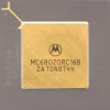
 
Last edited by a moderator:
Best part of going that route is that I'm heading toward doing the top part of that board for the 1400 already. I've been nibbling away at PBX' connections to the rest of the system since way back when hacks over on 'fritter was the place to be. 1400 (and 2300 by assumption) would be a split bus system. In the 1400 16bits head over to the board interconnect to the T-REX based Card Cage/I/R assembly and the other 16bits head in the opposite direction to the Video Card connector that's sometimes used for a NIC. I found a bit of my diagrammed documentation the other day. When things settle back down around here I'll have a look around the various HDDs and backups to see what I've still got.

I'm guessing Blackbird development followed closely along the lines of what had been established in the PowerBook Duo system. The Duo Docking Connector is a "Slot E" 68030 PDS implementation and the DuoDock is a multiple function expansion card at that  Slot Manager location. That would make the Ethernet and Video Out of the Blackbird the equivalent of an Ethernet MiniDock with its own compliment of 512K VRAM with the other 512K dedicated to CSC/LCD. Gotta take a good look at the DevNote when I get a chance, but that looks to me to be the way the Blackbird block diagram is heading.

Right now I'm trying to keep things simple. Like maybe prototyping the Slot B riser (and only Slot B for KISS compliance) to verify schematic development of that crazy 6400/6500 riser. ::)

 
I'd really like to see the support chips being used on the G3 upgrades that were made for the 1400. All the images I can find online for G3 Powerbook 1400 upgrades show the support chips covered by stickers, so I can't read what they say.
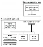
I'm not gonna touch the 466MHz/1MB Crescendo PB in Beater, but I've got a slower Sonnet G3 and one from NewerTech IIRC. Those I'll pull stickers from and shoot pictures of to your heart's content. But not gonna open up the 1400 stack storage box again until I finish getting the joint cleared out and a new roommate installed. [;)]

 
How's Plan A looking at this point? Mentions of "Plan B" always make me think of Demi Moore in the Charlie's Angels sequel. I love old Macs and terrible movies, puppies and kittens not so much  .  .  .  allergies!

 
Back
Top