• Hello MLAers! We've re-enabled auto-approval for accounts. If you are still waiting on account approval, please check this thread for more information.

PPC740L G3 CPU Daughterboard For Blackbird Powerbooks

Well, I think they're all waiting on me at this point, as I have to get my NuPowr (along with a logic board and display) to @Bolle somehow.

I believe Plan "A" is to swap a 740L in place of the 603ev that's on there now, and Plan "B" I guess is to fabricate a whole new CPU card with proper support for the 740L?

c
Yep, Plan A is the one we are working on now with the 740 and the NuPowr card. Plan A is currently looking very strong and promising. If for some reason we don't or can't anticipate a possible failure mode, then Plan B is indeed a whole new CPU daughterboard for the 740, with 32 MB of RAM. But Plan B would be a very long term project (+years) since it would require understanding the entire wiring of the CPU daughterboard and synthesizing a new one from that.

I'm not gonna touch the 466MHz/1MB Crescendo PB in Beater, but I've got a slower Sonnet G3 and one from NewerTech IIRC. Those I'll pull stickers from and shoot pictures of to your heart's content. But not gonna open up the 1400 stack storage box again until I finish getting the joint cleared out and a new roommate installed. [;)]
Sounds good, I look forward to getting those pics some time in the future.

 
Last edited by a moderator:
If you go to plan B, you might consider designing for a PPC750GX...
Good point. if we fell back to Plan B, I would probably target the PPC750FX instead since that was used by Apple, but the GX never was, so it's hard to say how difficult it would be to implement the GX without looking at the white papers for both and comparing their requirements.

We might also be limited to what the PBX can handle. The G3 upgrades for the PBX based systems was only done with the plain 750. Now whether that is a limitation of the PBX or just what chips were available at the time, it's hard to say. Considering the PBX is essentially a blackbox, it would have to actually be tested to determine if it could work or not.

 
Last edited by a moderator:
Since we're talking about Plan B: we were going over CPU choices in Franklinstein's 601 Proc Swap thread. I found 32,324 of the PPC750FX-GB1033T 733MHz BGA G3 available from AliExpress at $70 per. Trag had found a few different CPUs in small quantities somewhere else at better prices, but I figure availability is key. We're not gonna run out of the 733MHz FX variety anytime soon. The Blackbird and 1400 buses are 33MHz, the FX tops out at 666MHz for either. The bigger cache of the GX would be nice, but ISTR something about the FX being the last version with a simple PLL based clock multiplier setup. So I wonder about GX compatibility?

This stuff is more on topic in this thread, so here's the info I've dug up so far:

PPC750FX Evaluation Board User’s Manual

PowerPC 750FX Evaluation Kit Quick Setup for Windows

Migration from IBM 750FX to MPC7447A

MPC7447: Host Processor - NXP Documents Page

MPC7448 PowerPC® Processor

PowerPC 603e RISC Microprocessor Family: PID7t-603e Hardware Specification

PowerPC 603e™ RISC Microprocessor Family: MPC603r (Goldeneye) Part Number Specification

 
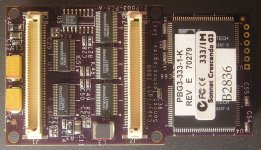
.  .  .  and the first installment of the pictures I promised:

Crescendo_PB_333-1MB-Sldr-a.JPG

Crescendo_PB_333-1MB-Comp-a.JPG

Couldn't resist a quick peek. Nothing of import under the stickers covering the SRAM and it's likely no mystery what's under the sticker topside, so I've left them on for now.

I'm thinking my proposed 1400/FX/666 board wouldn't amount to much more than what's on the Cache deprived 117MHz 603e board in the first release. Yours would amount to same with PBX underneath and built-in Max RAM expansion where the cache and controller are on this board.

 
Last edited by a moderator:
Good point. if we fell back to Plan B, I would probably target the PPC750FX instead since that was used by Apple, 

We might also be limited to what the PBX can handle. 
I don't think there's any functional difference between the fx and the gx interfaces, but I'm not certain.  Is the PBX that big ASIC on the upgrade or CPU cards?

 
Last edited by a moderator:
PBX is the Bus Bridge ASIC directly underneath the 603e on the solder sides of 5300 and 2300c and in the same place on the solder side of the mobo underneath the 1400's CPU Card connectors.

edit: does GX use PLL resistors in hardware for bus multiplier settings like the FX? If it's a later version, sounds like it's software only.

Paralel's pics on p.1 of the NewerTech NuPowr 167 MHz:

View attachment 25694

View attachment 25692

Looks like you can see the outline of PBX underneath the CPU in the box of vias surrounding it.

 
Last edited by a moderator:
Am I the only one here that has one of these upgrades?

It just occurred to me that these things are probably not the most common.

Also, if plan A is successful, I also realized that I'll have the only confirmed-to-exist G3-upgraded 540c :)

Maybe someone should try and find some schematics for these upgrades so we can replicate them!

c

 
Am I the only one here that has one of these upgrades?

It just occurred to me that these things are probably not the most common.

Also, if plan A is successful, I also realized that I'll have the only confirmed-to-exist G3-upgraded 540c :)

Maybe someone should try and find some schematics for these upgrades so we can replicate them!
I have a few different upgrades, from the original 100MHz part to the 183MHz version, but they work and I'm not ready to potentially ruin them through experimentation. Maybe if I successfully practice on a few 5500 boards, upgrading them with 300MHz 603es or 740s, I'll take the plunge on the considerably more compact and rarer 5x0 upgrade cards. If anybody has dead versions of the 5x0 upgrade I'll be happy to buy them for a reasonable price. Or dead 6400 boards; I need more high frequency (120MHz+) 603e QFPs for 23/53/1400 series upgrades and the blue epoxy IBM parts that I have are hard to rework.

Anyway supposedly the reason Newer didn't bring a 5x0 G3 upgrade to market is that the processor card connectors were discontinued and the molds were destroyed, either because AMP didn't want to keep them around or Apple requested their destruction (I lean toward the former more than the latter, which is a bit too conspiracy theory-ish though not entirely implausible given some of Apple's antics). So the only way Newer would have been able to make these cards would be for people to send their old cards in to have the connectors harvested. This would likely have been pretty expensive, and a good number of people would probably have preferred to keep their old cards as backups or for resale so would have been reluctant to send them off. Maybe if the internet were a bigger thing at the time it would have been easier to advertise and place orders for something like this, but internet shopping was still kind of niche and most people still ordered things out of catalogs so they probably just trashed the whole project because it wasn't viable. Either way, there's no way to get the connectors without destroying old processor cards, so new cards are unlikely to appear unless someone wants to sacrifice a bunch of existing ones. I suppose it's not a huge deal to harvest old cards anymore, seeing as many 5x0 series machines have fallen victim to either destroyed plastics or rotten LCDs.

 
I'd go with the the AMP marketing decision theory. The Blackbird's interconnect is a 16bit part given its pin count and it was a 32bit world by the time the G3 was released. The extra 10 pins on the the 1400 interconnect above would have made a significant difference by then, so why bother continuing production for a shrinking market with more capable parts going into production. Even the modem connector a couple of inches away on every Blackbird already had 100 pins at the same time.

I'll throw an the engineering decision theory as well to complicate the binary set. The 1400 part is far more robust than the Blackbird interconnect which suggests to me that even if AMP continued to produce an eighty pin part, they would have moved it into the same series as the 1400 form factor. Is the modem connector a 100 pin version of the 1400 interconnect? I put the Blackbird box away for the time being so I can't readily take a peek at a board.

For the EvilApple conspiracy theorists I'll make a point that would be more obvious to myself anyway. Apple likely used a part from an obsolescent series with a different height(?) for Modem and CPU interconnects intentionally. Such would make a unified bus processor card bridging both connectors nigh on impossible to implement. THAT would be just like something the denizens of the Infinite Loopiness would do. :P

edit: I don't have a Modem in my miscellaneous parts collection for the Blackbirds, can anyone prove or disprove the mismatched connector theory by telling me if the CPU and Modem  circuit boards are on the same plane? Also, if anyone has a spare modem card, I'd like to have one in my grubby little paws for testing the feasibility of a two connector PCB, mismatched or not.

 
Last edited by a moderator:
1400 (and 2300 by assumption) would be a split bus system. In the 1400 16bits head over to the board interconnect to the T-REX based Card Cage/I/R assembly and the other 16bits head in the opposite direction to the Video Card connector that's sometimes used for a NIC.
What? That's not how computer busses work.

 
.  .  .  and the first installment of the pictures I promised:

View attachment 25941

View attachment 25942

Couldn't resist a quick peek. Nothing of import under the stickers covering the SRAM and it's likely no mystery what's under the sticker topside, so I've left them on for now.

I'm thinking my proposed 1400/FX/666 board wouldn't amount to much more than what's on the Cache deprived 117MHz 603e board in the first release. Yours would amount to same with PBX underneath and built-in Max RAM expansion where the cache and controller are on this board.


What I find fascinating about this board is the lack of PBX ASIC. Is the PBX located on the logic board of the 1400? The developer note for the 1400 don't make it clear where the PBX is located for the 1400.

Am I the only one here that has one of these upgrades?

It just occurred to me that these things are probably not the most common.

Also, if plan A is successful, I also realized that I'll have the only confirmed-to-exist G3-upgraded 540c :)

Maybe someone should try and find some schematics for these upgrades so we can replicate them!

c
Of the NuPowr upgrades for the BlackBird, the 167 is the most common. There are about 15000 of them that were made and sold. Yours would be the 3rd I've seen

 
Last edited by a moderator:
15000 is quite a number.

But, if we're successful, there will still be exactly *one* such upgrade with a 740L installed [:D]

At least, one that we know of....

c

 
Last edited by a moderator:
15000 is quite a number.

But, if we're successful, there will still be exactly *one* such upgrade with a 740L installed [:D]

At least, one that we know of....

c
Yep, it would indeed be one of a kind.

I've looked into it fairly extensively. As far as I know. it has never been done before. The rumors of the Japanese guy appear to be confused with the guy that overclocked his 603.

 
Last edited by a moderator:
How much did you pay for the 740L we will be using for the... experiment?

Out of fairness, I should probably pay you for that if the upgrade works, since it will be going on my CPU card....

And then my part of the shipping, of course.

And Bolle's work?

Oh! And for anyone who might be interested, my NuPowr is 100% functional once again. Apparently the malfunction was caused by a bent pin in the RAM socket, which then shorted with an adjacent pin. It's fortunate it didn't fry anything!

c

 
What I find fascinating about this board is the lack of PBX ASIC. Is the PBX located on the logic board of the 1400? The developer note for the 1400 don't make it clear where the PBX is located for the 1400.
It would make sense for the PBX ASIC to be on the motherboard in the 1400, because unlike the "Blackbird" the RAM modules are also connected to separate slots on the motherboard, not hanging off the CPU card. Note that the card also doesn't have the ROM chips on it. So, in short, it looks like there's a lot "less of the computer" on the CPU card in a 1400 vs. a Blackbird. The two connectors on the bottom of the 1400 card are almost certainly little more than a buffered version of the CPU's direct pinout.

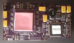
I'm going to hazard a guess that the mystery chip labeled "PBG3D" on that Sonnet 1400 upgrade are a cache controller for the SRAM chips; the 1400 originally didn't have a L2 cache.

 
What? That's not how computer busses work.
Could be wrong, usually am. But SCSC and the Video Card span displays, both limited to 16bits. That's why the unobtanium NewerTECH VIEWpowr 1400/16 is just that, limited to 16bits, that's what the connector speaks. I may not recall correctly, but in tracing lines from PBX on the 1400 logic board to the Video and Card Cage connectors (15 years ago) they appeared split left and right and to be a high/low type of thing. We're also not talking about any old normal computer bus here. The funky bridged 68030 NuBus architecture PowerBook I/O setup of everything from Blackbird up to the PCI architecture 3400 was a kluge from top to bottom  .  .  .

.  .  .  except for the Duo System, that was perfection! :lol:

 
Last edited by a moderator:
It would make sense for the PBX ASIC to be on the motherboard in the 1400, because unlike the "Blackbird" the RAM modules are also connected to separate slots on the motherboard, not hanging off the CPU card. Note that the card also doesn't have the ROM chips on it  <snip>   The two connectors on the bottom of the 1400 card are almost certainly little more than a buffered version of the CPU's direct pinout.
Exactly, PBX is located on the solder side of the 1400 board centered between the connectors above. Processor card interconnect is definitely a direct connection to the PBX Memory Controller/Bus Bridge which handles ROM, RAM and Expansion RAM on the Logic Board. PBX itself handles the buffering. I was surprised to see no additional buffering for the 1400, in the others the 603e and PBX are all but conjoined twins. 

I'm going to hazard a guess that the mystery chip labeled "PBG3D" on that Sonnet 1400 upgrade are a cache controller for the SRAM chips; the 1400 originally didn't have a L2 cache.
Yep, that's why I said there's probably no mystery about what's under the sticker. 133MHz and 166MHz processor cards w/cache have a similar setup. What the heck are those five ICs between the connectors on the Sonnet G3 board? I can't make heads or tails out of the designations  .  .  .  so I'm waiting for somebody who knows something about them to chime in. :approve:

So, in short, it looks like there's a lot "less of the computer" on the CPU card in a 1400 vs. a Blackbird.
Absolutely, that's why I'm targeting the 1400 processor card for a 666MHz FX build. Pretty much all needed would be the CPU, the specified resistors, capacitors and whatever voltage regulator black magic would be required. That's the recipe for the 117MHz Processor card:

View attachment 25631

View attachment 25630

Paralel, would shots of the 166MHz 1400 card be helpful for comparing it to the Sonnet G3 and the cache-deprived 117MHz card above? I may have a 133MHz card in the stack as well.

G, the 117MHz logic board is incompatible with either of the two later Processor Cards with Cache implemented. IIRC, the 133MHz Logic Board can be upgraded with the 166MHz Card. Might it be worthwhile to figure out why the 117MHz logic board is a special case? For the first release 117MHz logic board you have to go straight to a G3 upgrade.

 
Back
Top