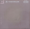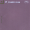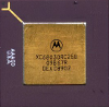
The "820-0961-A" mystery G3 3.3V FlashRom

Is there some way to tell the host machine which of those two addresses to use? The problem, that I see, is that the host machine expects the ROM to be at a certain address, and when it is programming the ROM, it's going to use those same addresses. Or do you get to choose the address range to which it programs?
It depends how many address bits exist at the ROM slot and how the G3 decides between built-in ROM and ROM DIMM slot.

The Beige G3 schematics is missing the page containing the built-in ROM chips? At least, I know sheet 9 is missing but that's for DRAM DIMMs.

Actually, does Beige G3 have built-in ROM chips? Gossamer HW ERS says no! So maybe forget everything I've been talking about...

The G3 schematics show the ROM DIMM is 64 bits (8 bytes) wide and has 20 address bits. I think that allows for 8 * 2^20 = 8 MiB of ROM.
If there's two banks then that's 16 MiB.

The MPC106 (Grackle) manual says:
For ROM/Flash support, the MPC106 provides 20 address bits (21 address bits for the 8-bit wide ROM interface), two bank selects, one output enable, and one Flash write enable. The 16-Mbyte system ROM space is subdivided into two 8-Mbyte banks. Bank 0 (selected by RCS0) is addressed from 0xFF80_0000 to 0xFFFF_FFFF. Bank 1 (selected by RCS1) is addressed from 0xFF00_0000 to 0xFF7F_FFFF. A configuration signal (FOE) sampled at reset, determines the bus width of the ROM or Flash device (8-bit or 64-bit) in bank 0. The data bus width for ROM bank 1 is always 64 bits. For systems using the 8-bit interface to bank 0, the ROM/Flash device must be connected to the most-significant byte lane of the data bus (DH[0–7]).

If the G3 doesn't have built-in ROM, then build a ROM DIMM that is 8 MB with a switch that selects which 4MB is at the FFC00000 range for boot?

We would have to change the programmer to program the FF800000 range or use the switch while the system is running which would probably be safe only for Open Firmware and in that case we would have to make our own Open Firmware programmer anyway.
 
It would be nice if the flash ROM had a switch to enable built-in ROM in case the flash ROM has a bug and needs to be reflashed. While in Open Firmware, the switch can be changed to expose the flash ROM for flashing.

Would it be possible to have a jumper or something on the flash ROM so that it appears as 4 MB at FF800000 instead of 4 MB at FFC00000 so that both ROMs can work at the same time? Then one can boot with the normal ROM to flash the flash ROM. This way, the switch doesn't need to be changed while the power is on to do a flash.
The way you would do this is put a switch that either connected to the most sig address line directly, or routed it through a NOT gate depending on switch position. That would swap the top and bottom half of the ROM depending on the switch position.
 
Actually, does Beige G3 have built-in ROM chips? Gossamer HW ERS says no! So maybe forget everything I've been talking about...
Correct. There is not built in ROM on the Beige G3. It's in the expansion slot, or not there at all.

Later Note: Most of the following discussion is entirely from my point of view regarding what I am getting ready to design/build. Discussing what could be done in theory is a related topic, but not one I focused on.

I think it is impractical to put 8 MB of Flash on a single module, or, more exactly, too expensive. I do not have any chips on hand that could do the job. It would require eight of these 44 pin PSOP chips and the module would need to be twice as tall. I guess eight 512K X 16 Flash chips in PLCC or TSOP package might do the trick. They're more compact.

Mouser is showing $7+ for 512K X 16 TSOP 5V flash. Interesting, they also have the M29F160FT55 (twice the capacity) for about the same price.

But then I'd have to completely redesign the PCB, which would be fun, but would mean I might not finish this year.

The other thing to consider is do you want a programmable module for the Beige G3, or for all the other machines that use this style ROM?

The Beige G3 uses 3.3V parts. The other machines (PowerSurge, NuBus PowerMac, ANS, PEx) all use 5V parts.

I am currently targeting a 5V module with a separate programming board that interfaces to the Xgecu TL866II+. I don't know if this approach will work or not, yet. It depends on whether the Xgecu has sufficient drive strength for the extra load, because the address and control pins are shared.

The modules I'm assembling for the ANS guys can be equipped with either 3.3V or 5V parts, but that's because they have 14 SM resistors for switching between the two voltages at assembly time. For the programmable module, I'm going to dispense with the resistors and recover the board space, and there will need to be two separate models of circuit board. This is not much of an issue now days because PCB fabrication has become so affordable.

Back when I did my original layout, pricing on PCBs ran something like $500 up front for tooling, and then a declining unit price for boards, depending on how many one ordered. I think the original 200 boards I ran off (in 2003) cost something like $1700. So there was a lot of motivation to make one design do everything.

Anyway, my hope is for a programming board (in concert with an Xgecu) that will work with both types of module, but two different module designs for Beige G3 and other. I was hoping to combine to just one module design with all power pins always connected (both 3.3 and 5V) because it seemed that a host machine must supply either 3.3V or 5V. But the schematic for the Beige G3 shows the monster giving the ROM slot both 3.3V and 5V, so if I tied those pins together, that would be bad.

Finally, because my new module will connect the WE_ and Reset_ pins to the module, it should be possible to write a routine for in system programming, if your routine can run without reading the ROM at the same time, but the Ready/Busy pins will be unavailable. I can/will run them to the DIMM edge, but the Macintosh architecture doesn't have any connections for them.
 
Last edited:
Back
Top