• Hello MLAers! We've re-enabled auto-approval for accounts. If you are still waiting on account approval, please check this thread for more information.

Macintosh Plus Internal Hard Drive *Mod*

Oh man, jt is starting to have an identity crisis...
I dunno why he's rambling about this, tbh. I've addressed him as JT in other posts, and in PMs, and he's never made a stink about it. I figure just as long as you don't address him by his full username, you should be OK.

 
I was responding more to uniserver since he had jt's name huge in all caps just after he said to use lower case, but the original post has since been edited.

thanks

JT
 
No, stink . . . it's no big deal, Concorde. I thought the juxtaposition was hilarious, so the }:) made me do it!

I'm a tad sleep deprived the last few days, so I'm reverting to the lowest forms of humor, it's fun . . . aside from the pun.

Chalk it all up to:

THX, bro, I needed a laugh!
/fun-n-games!

Back on topic:

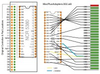
@ uniserver: the mistake I made was connecting /RST on the ribbon cable to TRST on the IC rather than RST, other than that, it looks to me like you're good to go.

If I'm interpreting the transition correctly . . . if I flip the cable across to the other side of the controller and roll it over, my diagram should match the pretty colored one. That way DB0 will be the only data line crossing the other 7.

Rotating the IDC header on the PCB so that the ground strip faces the Controller IC ought to simplify that layout when the time comes.

@tt: how critical do you think trace length will be for my PCB IC->50 pin IDC header Adapter? I'm going to try counting the tick marks on dashed lines in AI to roughly equalize trace lengths, then have someone do a "real" PCB layout for seeeding some boards.
@ dougg3 & bbraun: will the conversion PCB for the ROM SIMM help to increase the size of the Addressable ROM space or just make it possible to use the ROM SIMM for ROMswappin-n- hackin' the Compact series . . . or neither?

 
PCB layout follow on questions:

1) Do any of the available programs have an auto-meandering for automagically equalizing trace lengths while autorouting?

2) If I do roughly meandered trace lengths manually via wetware in AI, will an available program do auto equalization?

3) Will an available program at least read out total trace lengths of a manually meandered PCB layout for manual tweaking?

4) If 1) are my requirements so basic that using machine AI routines be feasible rather than this old fart, farting around in AI9?

Lazy minds want to know! :approve:

 
@ dougg3 & bbraun: will the conversion PCB for the ROM SIMM help to increase the size of the Addressable ROM space or just make it possible to use the ROM SIMM for ROMswappin-n- hackin' the Compact series . . . or neither?
Um... What? I'm not sure what you mean by conversion PCB. AFAICT from the drawing above, you're talking about making a ROM SIMM that takes DIP sockets instead of PLCC?

Or are you trying to get something that plugs into the DIP sockets on the logic board that you can also put the ROM SIMM on? I'm not sure how that would work physically, but... The compacts have 2 8bit DIP PROMs that are have data interleaved between them so it produces a 16bit word on the 16bit bus. As opposed to the 32bit bus the ROM SIMM sits on. So, I guess it could work, you're just not using half the ROM SIMM capacity. But you're still limited to the address lines available to the sockets you're plugging into.

If you wanted to go soldering wires all over the place to get additional address lines, the 24bit addressing of the 68000's is pretty forgiving as I understand it. There's no MMU to worry about address spaces being mapped appropriately. All bus accesses appear to be "successful", as in you don't have to worry about the memory controller generating bus errors for certain address ranges. So basically you just sit on the bus and either put data out or not whenever you want. Which is why they rather literally just have those two PROMs sitting directly on the bus without any need to generate tri-stated acknowledge signals or anything like I had to worry about on the PDS card.

So ROM size is limited only by the address map. Pre-Plus systems have 5MB of contiguous address space available from the start of ROM until you hit the SCC registers. Plus systems are much more cramped at about 1.5MB because they threw the SCSI controller in there.

 
@tt: how critical do you think trace length will be for my PCB IC->50 pin IDC header Adapter? I'm going to try counting the tick marks on dashed lines in AI to roughly equalize trace lengths, then have someone do a "real" PCB layout for seeeding some boards.
I am no expert, but I am guessing if the trace lengths are different say on the order of 1-2cm, there will be no impact to the timings, etc., hence no need to worry about them. The main thing is having a schematic and ready-made parts available in a standard library (if using Eagle CAD). If those are available in Eagle CAD, which they probably are, then making that design would not be too difficult.

 
:lol: Parts? What parts?

Try a 50pin DIP header and a 40 pin DIP socket on for size! One of the pairs of socket thru holes will really be for, single row, 20 contact, downward pointing DIP headers. They'll be for soldering the adapter PCB to the MoBo's through holes for the SCSI Controller. Maybe I will use a socket for the Controller IC, but the header will be of the shrouded, keyed, ejector winged variety if I have enough wiggle room front to back.

Heck, I can get 'em within that margin of error with standard equipment, Mark I eyeballs . . .

. . . no need to count dashes! [}:)] ]'>

But I'll do so anyway! :approve:

 
@ bbraun, thanks for the reply, guy. I missed it while snoozing during the page-break. Yes indeed, I'm aiming at pluggin' a PCB into the existing ROM Sockets with a ROM SIMM socket on board. The clearances between my MicroMac 68030 Accelerator and that stupidly positioned MoBo<->A/B Cable Connector look like they might work out for the second/third adapter board to add to that 68030 Card in my onetime-128k.

Once my brain fires up again, if ever, I'll take a stab at divining the implications of what you seem to have outlined after I re-parse the .TXT.

At first run, it looks like running some line or other to the adapter ought to make the other half of the SIMM's 32bit word accessible as another 16bit word by flippin' an A/B gate.

Will Compact Virtual run on the Plus? Sounds like adding some SRAM to the adapter board might prove interesting in that case.

< so to speak. }:) >

 
Fresh out of AI9:

MacPlusAdapters.002.2p.jpg

I've noted the error in yellow and the correction in blue. If there are no objections, you're probably good to go, uniserver.

I've changed the PCB's Ribbon Cable connector orientation. Dunno if it makes sense for layout, but if I don't have room for the keyed shroud, ejector arm connector, at least the key on the cable connector is pointing at the Controller IC rather than aimed where it can interfere with the backside of the DB-25 connector housing.

 
NoPro, glad to help out . . . hope it actually helps . . .

. . . somebody PLEASE give it a look over to check for errors.

Specifically, make sure I transcribed the pinouts correctly from the info linked above and against other sources.

MacPlusCSCI_PCB.2p.jpg

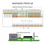
I wasn't sure . . . well . . . I was fairly certain that very few were visualizing what the heck this PCB layout is all about, so:

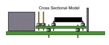
I did a quick illustration to show how it shoehorns a 50 pin IDC header in between the SCSI Controller's original position and the back side of the SCSI Connector by shifting the controller toward the "fence/ground bar" of the Plus Mobo. Sourcing a new SCSI Controller makes it a snap, just grind the legs away from the original IC and then desolder each pin individually from the MoBo. The PCB has standard square header rows soldered to top and bottom. the double row for the internal SCSI cable is on the"component side" and two shorter, single rows are soldered to the "solder side" of the adapter. These will be soldered into the thru-holes in the MoBo vacated by the Controller IC's legs, then clipped.

@ PCB designers: How many traces will I be able to run between highway between the header rows? I can always plan on using some patch wires between vias, so this shouldn't be terribly difficult to get it laid out. [:)] ]'>

I haven't shown them for clarity, but I'll be using a pair of single row machine pin sockets so the new SCSI Controller IC is removable in case any of the solder joints under it ever need rework.

Measurements are not to scale, clearances are considerably tighter than shown in the illustration, but doable! [}:)] ]'>

 
THX, Charles, I think it might work out to being a bit easier to do and far more robust than what's gone before.

Spotted a boo-boo already, easy fix though. GND got mixed up with /ATN . . . I'm still sleep deprived. :-/

I'm almost tempted to do all the connections that don't come out to within a mm (or four) of equal lengths with patch wires for equalization. Just run 'em underneath the socketed controller so they're maintainable and nobody'd be the wiser! Cheat neat! [}:)] ]'>

 
Nice mock-up jt! You might also want to add a view with the connector body from the cable to see if it fits in the space.

A killy clippy thingy would be cool too, so no board mod would be required. Maybe with that design it would be a double decker PCB: headers on either side of the chip acting as pillars to the second PCB with with the 50pin header in the middle, but maybe that would end up being too tall.

 
K.I.S.S. live by it!

Fixed the boo-boo & didn't stop . . . |)

MacPlusCSCSI_PCB.2p3.jpg

I think it's laid out, but I'll need to review it when I'm relatively conscious again . . .

I need to "cut the corner" on lines DB1-DB7 to keep those traces as close to the length of the DB0 trace as possible.

No biggie, but I'd appreciate some feedback on accuracy of the pinouts and trace routing aforehand, gang. TIA.

I've got six jumper wires (yellow pads) designed in to lengthen the signals bunched up in the center . . . makes it better . . . and easier . . .

. . . and they're ALL hidden underneath the socketed SCSI Controller IC. [:D] ]'>

+InternalSCSIconverterPCB2.jpg

zzzzzzzzzzzzzzzzzzzzzzzzzzz xx(

 
K.I.S.S. live by it!//
You have gone way beyond that so far though... Get a nice rainbow ribbon, solder the wires and you are done. It can have a male socket at the other end if you want it connectorized.

 
Yep, you got me there! Nice depth charging, I'm sunk. My only excuse was that I was sleep deprived during this entire Rube Goldberg inspired design session.

One full four hour sleep cycle and a nap after work takes a hefty toll after four days. xx(

I should have realized I was heading over the top when I saw that only two wires needed to be soldered next to that blasted stiffening bar/fence. I almost figured that out when I had to resort to patch wiring to get the PCB layout close to what I wanted. I really dislike the Idea of having wiring soldered to an IC in such a way that I'd be hesitant to remove the MoBo for fear of pulling something loose. So the patch wiring under the socketed controller didn't really bother me, no stresses under there.

Now that you've pointed out the complexity of the PCB hacking process (and getting my first full night's sleep since Saturday) I may have come up with a fairly simple approach that adds adequate strain relief to the direct solder process. I'll work the kinks out of it and post another variation on the ribbon cable diagram, maybe while I'm flip & flopping the graphic for clarity and comparison to the existing diagram.

There's no need to source that garishly colored ribbon cable, BTW. It overpowers the natural beauty of the colors on the A/B, CRT, chassis and MoBo, IMHO. Just use a continuity tester before soldering any wire to verify you've got the correct one! Test twice, solder once: K.I.S.S. [:)] ]'>

.TXT version of the tt inspired variation on the direct approach:

The alternate cable adaptation involves wrapping and soldering all 24 alternate ground lines around a piece of fairly stiff copper wire and then hot gluing that assembly into the groove on the "back side" of the ground bar/board stiffener. The red ground wire is left longer, with the insualtion removed from a section wrapped and soldered to the tie wire. the red wire is stripped and soldered to any handy point on the MoBo. The thruhole tying the A/B connector's ground line on the solder side to the ground bar on the component side at R15 looks like a nice place to wick out the solder. Stick the stripped red wire through to the solder side and then re-solder the original connection from the solder side so it almost looks like it was planned for the red wire to be terminated there. [}:)] ]'>

The kicker to this process is to pass all the prepped signal wires and four discrete ground wires underneath the stiffener bar before soldering them onto the legs of the Controller IC. Presto, Instant strain relief! Slack will be dotted randomly to keep the intentionally messy wire monster down there in the NCR_5380_Crevasse. No worries about sliding the MoBo in-n-out doing it that way. An artful random tacking of the signal wires down in there will prevent crosstalk at the same time. Splicing the four discrete ground lines together and shrink wrapping the connection with a single wire emerging to be soldered to GND on the Controller would be elegant, especially if both ends of the shrink wrap are hot glued somewhere that the bonus underbar strain relief down in the crevasse side of the ground bar/stiffener looks attractive.

Moral of this silly story: If you can't quite make it far enough over the top to clear the razor wire doin' a Fosberry flop and wind up landing near your takeoff point, just drag that shredded bloody butt very gingerly underneath that #@^%$#^% fence! [:o)] ]'>

THX for the wakeup call, tt! U b 8-) :approve:

< shakes a couple of loose cobwebs out of skull and fires up AI9 once more . . . >

p.s. We can reduce the fence side soldering to just the /RST line if we find the correct value resistor at/near R15 and repeat the red wire MoBo dive to the solder side trick at the resistor's thruhole connection with the VDD (VCC?) line if it's electrically permissible . . . [}:)] ]'>

 
Back
Top