-
 Hello Guest! We're hosting a challenge to welcome vintage Intel macs to the MLA during the month of July! See this thread for more information.
 -
We've made some quality of life improvements to the Trading Post. More info here.
You are using an out of date browser. It may not display this or other websites correctly.
You should upgrade or use an alternative browser.
You should upgrade or use an alternative browser.
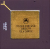
IIci cache card re-creation
- Thread starter rieSha.
- Start date

Not aware of one, feel free to take this on 

This one looks quite cloneable: https://ebay.us/m/wWMbtC
I don't think anyone's bothered. Micron has a 128K cache card that is just GALs and discrete logic, definitely clonable. However, it requires TAG SRAM which can be difficult to come by.
Overally though cloning a cache card is a bit of a "why bother" as the improvement is very incremental. A simple 030 clock doubler accelerator would give greater performance at a similar cost. I don't have much interest in the IIci though so haven't done more than some testing in IIsi.
Overally though cloning a cache card is a bit of a "why bother" as the improvement is very incremental. A simple 030 clock doubler accelerator would give greater performance at a similar cost. I don't have much interest in the IIci though so haven't done more than some testing in IIsi.
Depends... back in the days when I ran a IIci under NetBSD as my home server, I saw a 30% performance improvement.Overally though cloning a cache card is a bit of a "why bother" as the improvement is very incremental. A simple 030 clock doubler accelerator would give greater performance at a similar cost. I don't have much interest in the IIci though so haven't done more than some testing in IIsi.
A 68030 clock doubler achieves 100% improvement best case, 60% on typical performance trace, and a minimum of 10% on worst case. Cache achieves about 30% in best case scenarios (memory bound) and 0% or sometimes negative in worst case.Depends... back in the days when I ran a IIci under NetBSD as my home server, I saw a 30% performance improvement.
Given similar costs for BOM, this hypothetical (cache-less) accelerator works out to better bang for the buck. Not that cache doesn't have a benefit, but it's most effective when increasing the CPU clockspeed.
Yes, tag SRAM (which include comparators so they can do both storing and checking of tags) haven't been made in years, are expensive if you can find them, and won't help making bigger/better caches. Using a programmable device (i.e. FPGA) with embedded SRAM for tags (and external discrete SRAM for data) is theoretically possible, but would make for an expensive cache as you would need a fairly large FPGA just to get enough embedded SRAM for the tags.I don't think anyone's bothered. Micron has a 128K cache card that is just GALs and discrete logic, definitely clonable. However, it requires TAG SRAM which can be difficult to come by.
Also, the best an external cache can do is 2-1-1-1 burst (which may or may not offer benefits over non-burst 2+2+2+2 timings, which is equally as hard to achieve timing-wise). If your memory can already achieve that, then a cache is pointless (and in fact will make things worse by slowing things on a miss). And while it's closed-source (so it can't be easily reworked for a different machine) and somewhat expensive, the Synchr030/S proves it can be done for the 16 MHz '030 in a SE/30 using 'modern' components. The best option for a IIci (or any '030 machine!) would be to have something similar, negating the need for a cache. Even if only 3-1-1-1 burst could be achieved on faster '030 with SRAM, and external cache would likely still be useless.
Yeah, the TAG SRAM is a big stumbling point for accelerators targeting machines of this vintage. Especially at high speed operation there's not much of a choice as unless you've an extremely fast SRAM and comparator it's going to be slower than a dedicated TAG which I usually get a match/no match decision faster than the rated speed. The 12ns TAGs I'm using on the Hyperdrive accelerator usually have a valid result by 8ns and definitely at 10ns. Impossible to beat in discrete logic. I was thinking to possibly adopt some of the later Pentium TAGs if I need to increase the cache size, or a FPGA. As you said it becomes fairly awful though as you'd need a largish FPGA and level shifters....Yes, tag SRAM (which include comparators so they can do both storing and checking of tags) haven't been made in years, are expensive if you can find them, and won't help making bigger/better caches. Using a programmable device (i.e. FPGA) with embedded SRAM for tags (and external discrete SRAM for data) is theoretically possible, but would make for an expensive cache as you would need a fairly large FPGA just to get enough embedded SRAM for the tags.
Also, the best an external cache can do is 2-1-1-1 burst (which may or may not offer benefits over non-burst 2+2+2+2 timings, which is equally as hard to achieve timing-wise). If your memory can already achieve that, then a cache is pointless (and in fact will make things worse by slowing things on a miss). And while it's closed-source (so it can't be easily reworked for a different machine) and somewhat expensive, the Synchr030/S proves it can be done for the 16 MHz '030 in a SE/30 using 'modern' components. The best option for a IIci (or any '030 machine!) would be to have something similar, negating the need for a cache. Even if only 3-1-1-1 burst could be achieved on faster '030 with SRAM, and external cache would likely still be useless.
The 030 synchronous cycle is annoying. At the clocks the cache cards operate at, 2-1-1-1 bursts or constant 2 cycle non-bursts I think is a wash in terms of effectiveness. On the Diimo 030 at 40mhz last I looked it exclusively used two cycle accesses despite having the logic to support burst operation. Either way the cache cards could easily do 2-1-1-1 or 2 cycle with SRAM, but that's much harder with DRAM. I've been flirting with the idea of sticking 16MB of SRAM on a booster just to see how fast an 030 operating entirely out of SRAM could be, with ~15ns SRAM 0 waits should be doable at 50mhz. Of course, the local-fast-ram approach only works easily if you're willing to forsake DMA access and the fancy NuBus cards that do DMA.
Still on the to-do list is to investigate how frequently the cache maintenance traps are actually used. The IIci cache slot has a few lines to allow access to the TAGs and perform flushes, etc. But I am not sure they actually do much more than enable the cache and call it a day. The Diimo 030 accelerator definitely snoops external accesses, I never did check if it fully snoops them or if it just invalidates though.
I've adopted the invalidation approach on my 040 accelerator where software must invalidate deliberately cache lines that reside in an address range that is cachable. Certainly, it seems fine in a LC475 without any special treatment at the moment even with DMA in play. Seems like DMA buffers are also allocated in non-cachable ranges too. I'm primarily targeting NeXT though which does not do that, and eventually I'd see this design as a possibility for the quadras stuck at 25mhz.
Did you find a viable option? At 5V, 16 Mbit SRAM are expensive and with big MOQ, while 4 Mbit are more viable but you'd need 32 of them - that's a large PCB, and I'm not sure what the signal integrity would look like with all those extra chips/traces. I've thought about it as well, but couldn't find a satisfying design trade-off.I've been flirting with the idea of sticking 16MB of SRAM on a booster just to see how fast an 030 operating entirely out of SRAM could be, with ~15ns SRAM 0 waits should be doable at 50mhz.
PSRAM are cheaper for the capacity, but much slower are 70ns for those available. Maybe for slower-clocked '020/'030, but not for fast ones. And they are 3.3V so the level shifters rear their expensive heads again.
Ultimately, fast (but not necessarily big) FPGA + SDRAM is likely the most appropriate solution for fast memory on a '020/'030 (still with some shifters). I might have a shot at that one someday, though probably not targeting speed at all cost (the Synchr030/S needs access to /ECS to get maximum performance, but it's not available on the PDS so it's a bit hackish).
Mmm, does the NuBus controller has the memory timings of the host memory controller baked in so that using different ones would be an issue ? Assuming it's IIsi or later and using /STERM couldn't it adapt to faster turnaround ? (... I'm not sure on which side of the fence the IIci is falling actually, if it's /DSACK only then 3-cycles and no burst at best).Of course, the local-fast-ram approach only works easily if you're willing to forsake DMA access and the fancy NuBus cards that do DMA.
No, that was part of it - not really any viable options unless we're overvolting 3.3v SRAMs or looking at limited availability/expensive chips. For my purposes I treated more than 8 SRAMs as being problematically complex. Doing 3.3v properly would be a double-whammy as you'd need a buffered high-speed 5v domain for at least the data bus as well as a 3.3v domain connected to that. Either way you're committed to 4 bus transceivers at minimum, and probably at least 8 SRAM chips for a 5v-only design. It gets out of control fast. I concur that a high speed DRAM based design would be the more viable choice. I'd be curious if any of the amiga folks have done local DRAM + 030 as DRAM+040 is common combo for amiga accelerators.Did you find a viable option? At 5V, 16 Mbit SRAM are expensive and with big MOQ, while 4 Mbit are more viable but you'd need 32 of them - that's a large PCB, and I'm not sure what the signal integrity would look like with all those extra chips/traces. I've thought about it as well, but couldn't find a satisfying design trade-off.
PSRAM are cheaper for the capacity, but much slower are 70ns for those available. Maybe for slower-clocked '020/'030, but not for fast ones. And they are 3.3V so the level shifters rear their expensive heads again.
Ultimately, fast (but not necessarily big) FPGA + SDRAM is likely the most appropriate solution for fast memory on a '020/'030 (still with some shifters). I might have a shot at that one someday, though probably not targeting speed at all cost (the Synchr030/S needs access to /ECS to get maximum performance, but it's not available on the PDS so it's a bit hackish).
Mmm, does the NuBus controller has the memory timings of the host memory controller baked in so that using different ones would be an issue ? Assuming it's IIsi or later and using /STERM couldn't it adapt to faster turnaround ? (... I'm not sure on which side of the fence the IIci is falling actually, if it's /DSACK only then 3-cycles and no burst at best).
IIsi uses same chipset as IIci. Or rather the inverse. The nubus controller respects whatever timings, so that's less of the issue, biggest problem is with the video buffer living in main RAM of arbitrary length you run into pretty nasty problems if you wanted to holepunch to allow that to work. The readout path for that is hardwired so you'd preclude the use of onboard video entirely otherwise. Massive headache.
Second part is for maximum speed you want the fast ram to be on the high speed bus, but if you have to be able to respond to external cycles from a true alternate master (integrated video is not) you get a nasty spike in logic complexity settings things up so that the external slow bus can access/drive the local high speed buses and appropriately generate strobes/acks. Eugh.
That said proper DMA is uncommon in 68k Macs and mostly limited to high end cards like the fancy SCSI boards, Radius rocket, and possibly some of the exotic interfaces (audio, etc). So the loss wouldn't be the end of the world and for example the LC475 works perfectly with bus arbitration disabled, except for an Apple-branded LC PDS ethernet board that does DMA. I'm thinking if I do a Mac version of the 040 HyperDrive, I may have a jumper to disable arbitration as the 040-style arbitration comes at a cost to speed.
I'd be curious if some of the exotic apple nubus cards like the Ethernet NB and 8*24 GC utilize DMA to main memory.... 8*24 GC definitely could master to other cards, not sure about main memory.
Similar threads
- Replies
- 0
- Views
- 180
- Replies
- 7
- Views
- 980
- Replies
- 16
- Views
- 2K