• Hello MLAers! We've re-enabled auto-approval for accounts. If you are still waiting on account approval, please check this thread for more information.

Farallon ETHERMAC LC NSC w/NuBus drivers in the SE/30 PDS?

When all you have is a great big bag of hammers  .  .  .

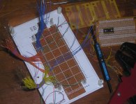
All connections have been unwrapped, clipped to length and stripped. Errant graffiti cleaned off the board and it's ready to go for round two  .  .  .  AFTER I finish the homework. ::)

strippeddownnreadytorock.JPG

Tried to use the cheapo stripper on the right and went back to the one on the wrap tool after borking a couple of wires. They've been replaced and I'm looking at how best to use a section of the Perf/PCB with the socket on it as a daughtercard for the inverter setup.

 
Well, it looks like you got the hard part done, now all that is left is the fun part :cool: If there is anything I can do to help, please let me know.

 
Fun part has already started. I ordered a quartet of 74LS04 inverters last night. I've spent the morning prepping the board for installing headers and socket directly to it w/o any possible electrical contact to adhesive residue.

-  gunk removed with good ole' WD40

-  cleaned that residue up with isopropyl alcohol

-  drilled out the perf holes so the thicker standoff base of the socket make no contact

-  used a larger drill bit to countersink the holes on both sides to remove copper and FRP surfaces for insurance

-  drilled out the perf holes again for the socket with a larger bit adding yet more clearance. That should ensure the holes are bare FRP with no possibility of contamination duing previous steps

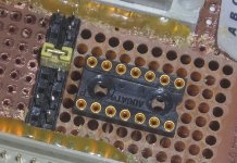
-  set up the two rows of long headers so they're configured in triads as above with gaps in the pins so no arrangement of headers can short address lines

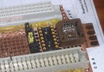
Socket-Headers-Inverter-1.JPG

There are plenty of holes cleared in case we need a more complex logical intervention. A 20 pin socket can be installed or beaucoups headers if more contacts might be needed for installing a daughtercard. Outside of a tiny blister trying to develop on my thumb from manually twisting the bit in countersinking all those holes, all is good. Due diligence time, back to doing homework for error checking when I get a chance. I've got SAT/SUN off for a bit of wire wrapping playtime if all works out. [:)]

Is crazy glue gel electrically conductive at the digital logic level or is it an insulator?

edit: hot glue or epoxy?

 
Last edited by a moderator:
I actually just ordered one of those AUGAT connectors for the 74LS04 chips I have.  This way if we make progress with the SE/30 I can working wrapping the SE version.  Looking forward to seeing what happens by this weekend ;)

 
Lots of homework to be done for that project before you start playing with the cool new toys! [;)]

68020 <-> 68030 - seemed straightforward enough for me to have at it

68020 <-> 68000 - not so sure about that one, you can color me clueless

One great thing about your SE hack: AFAIK the SE doesn't have a clue about Slot Manager and the Slot E conflict complications it brings to the SE/30. The SE PDS does its own thing and the video subsystem hasn't got a care in the world when it comes to its operation IIRC. But as I said, I'm pretty much clueless.

If you wanna take a stab at it I'd suggest starting up a dedicated thread. Folks will jump in to help you out on that project. I've floated too many whack-doodle notions here, so my byline tends to get ignored. :mellow:

 
Clueless here about digital design as well, so I've been asking around for help in getting a handle on it. This came up in the discussion. Don't claim to understand it, but I can draw pretty pictures about it. ::)

View attachment 27571

This way the shorted line for direct, non-inverted connection is on the input side of the inverter. Having it on the output side might be a problem? Is the 04 output tri-stated to give a null connection on output side with no input? Also unsure which PDS gets hooked up to the inverter input, guessing the LC PDS as in the bottom half of my diagram?

View attachment 27536

Totally confuzzled here and I probably got  the diagram all wrong too. :mellow:

 
Last edited by a moderator:
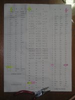
@maceffects Here's how to go about checking my wrap map and how to go about starting one for your SE Adapter. This one has been kicking around in my pocket:

Wrap-Map-HowTo.JPG

To create the map:

1 - Choose a pin location on the LC PDS' pinout grid, in this case Row 30 in column C is A19 (signal and coordinates highlighted in yellow)

2 - Identify C30 in the wrap map sheet in the center and mark it with a dot (also highlighted in yellow) Table is natively LC PDS format.

3 - Identify signal A19 on the 030 PDS and mark it with a dot

4 - Read off column and row location of A19 on the 030 PDS (highlighted in pink)

4 - A19 also happens to be in Column C on the 030 PDS, but it's on Row 29

5 - Go back to the dot at C30 on the wrap map and enter C29 (in pink here, pencil is editable)

To proofread/error check my new wrap map, work from the paired grid locations of the wrap map in the center. Read print at grid locations on LC and O30 sides, compare them to make sure the .TXT is identical on both sides.

Doesn't matter what the signal themselves are, just the .TXT string. It's maybe a bit like working backwards from One-Time Pad Code using DCaDftMF pinouts with an oddball offset table cypher twist to it? What goes into one side of the wrap map substitution table needs to come out in plain text on the other. The trick is to build the substitution key correctly so the wires can be plugged into the switchboard for proper communications between the two sides. I'm sure there's a far more simple explanation for the type of encoding this is, but that's the image that popped up in my head.

 
I just knew I screwed it all up!

View attachment 27579

This might be better. It would have parallel lines heading to the 030 this way, so I'd gate them to a single line with another jumper block. Still trying to get a handle on this so I've built a worksheet. The fluidic computing model in my head doesn't translate well at all to digital logic it would seem.

Any help from anywhere would be greatly appreciated. I'm sure Bolle's many projects keep him too busy for a primary ed course. Gotta see if I can grok the CMOS Cookbook on another pass. Would the earlier TTL Cookbook be better as a primer?

In Bolle's diagram, I just can't get the notion that the shunt is supporting a column of water in the inverter out of my head. :-/

View attachment 27536

 
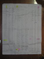
Thanks, here's the finished first draft from yesterday. If you or anyone else could check it for errors using the instructions in the post above it would be much appreciated.

RoughWrapMap2.JPG

Here's what I'm planning for the Logic at this point. Not crazy about having two wires coming to the block from each address pin on the 030 PDS, but this is what I can do without adding another jumper block trio to neck it down to one wire:

View attachment 27658

Thinking in .TXT:

First test:

No connections to 74LS04

Yellow from LC PDS address lines implemented

Light brown non-inverted signals implemented

All three jumpers completing the circuit

Expected result: HARD fail in this config, it will be overwriting Video Memory space in the SE/30 unless the video subsystem runs within  the high order bits? NIC uses A1-A16*****

Second test:

Unwrap the temporary (purposely left longer} wire for 030 PDS A22 from the jumper block, cut, re-strip and wrap it it to the header on the jumper block for Pin 8 Y4

-  at this point I could just direct connect the A22 lines for inversion on the 74LS04 socket as it will always need to be inverted? Food for thought.

If the card looks like it's starting to work in SlotID $A

-  I can put off messing with the other two address lines. They're there in reserve in the case that we need to implement the NIC in the NuBus Slot Space of the IIsi: SlotID $9.

Hail Mary:

Give up on $A and beat the snot outta every conceivable $9 setup, including variations on the /NUBUS signal of the 030 PDS.

Time for me to check the rough map as I transcribe it into the AI file. Little outside help with the error checking please?

edit: hrmmm ***** Video in Slot $E of the IIsi and the SE/30 use A1-A16 I've got another silly notion. If nothing else works, might it be possible to redirect addressing of the NIC to A17-A31 in the Slot $E space without conflict?

 
Last edited by a moderator:
Meh... went through DCADFTMF again.

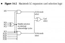
We might need to decode some more address lines to generate the /FC3 signal that tells LCPDS cards the addressing mode.

I did not know about that one earlier, so our test card might still be doing 32bit addressing, it just didn't look like it does from just looking at the used address lines.

Maybe we will have to take a step back and test the card what mode it is using. If it is indeed running in 24bit mode only we are fine with what we got so far.

If it is switching modes we need to implement some logic to decode the 32bit address range and set the /FC3 bit accordingly so that the address decoder on the card can actually be fooled to generate a card select signal.

We will have to watch address bits from 20 to 31 to see what's going on.

This is what every LCPDS card should be doing:

Bildschirmfoto 2019-05-05 um 14.32.15.png

We will have to run address lines 20 to 31 through a GAL and generate:

-A22 (inverted for 24bit mode)

-A26 (inverted for 32bit mode)

-/FC3 (for the address decoder on the LCPDS card to work)

We have to pick up on: (high to low - assuming slot A)

1111 1010 0000 for 32bit mode ->/FC3 high, A26 inverted, A22 normal

0000 0000 1010 for 24bit mode ->/FC3 low, A26 doesn't matter, A22 inverted

Gotta get my LC out of the basement and check if my Asante LCPDS NIC does mode switching or not.

 
Last edited by a moderator:
Damn! I was wondering about FC3 not swinging in the breeze? If It's just the one signal, all is not necessarily lost.  Can I re-wrap my board with /FC3 hardwired for 24bit mode with  the SE/30 running in same? We should get a yea or nay on the adaptation before developing your decoding logic, no? I've got a tube of 20 pin thruhole GAL sockets I can wrap on hand when the time comes. I'll drill a row or three more holes for one on the edge of the perf before I start wrapping anything.

Silver lining to this cloud: you figured this out while I was sleeping. I was excited about using epoxy or superglue to set headers and socket in place to start wrapping today. They'd have been in the wrong place as well. Any chance we'll be using my new jumper block config for anything in the next step? I thought that one was pretty cool last night.  :mellow:

I'v also got a 28 pin wire wrap socket or two on hand and some 35mm x 45mm breadboards with DS tape on the back I can stick to the perf board edge leaving my cleaned up section free and clear. I'll drill two or three more rows of holes on the edge to fit the GAL socket to the board with header blocks and DIP socket already in place. Will our three spare inverters be sufficient? 

Lemme know if the 24 bit gambit is worth pursuing and I'll just wrap the headers and socket in place.

 
Last edited by a moderator:
Hooked up the LA to the card in the LC... it looks like my Asante card is running in the same mode as the machine is set to with no mode switches when the card is accessed.

When in 24bit mode all I get are interrupt acknowledge cycles (FC0, FC1, FC2 -> 111) while A31 and /FC3 are high.

Lots of action on the select criteria for slot E in the 24bit range though.

So I would say if we stick to 24bit mode for now we should be cool (if your Farallon card/driver behaves the same way as my Asante seems to do)

Put /FC3 to ground and see what happens when wiring up the rest as planned before.

 
Last edited by a moderator:
That's good news all around. Found the GAL sockets, no need to risk further stress on my the wrap by drilling any new holes in the board.

Headers-Inverter-GAL.JPG

Also, the two header strips I had prepped will work hooked up inline without any chance of cross wiring the jumpers. [:)]

edit: I think I'll test all the re-stripped wires for continuity from wrap to socket before I start. I can get the inverter setup done while somebody checks my new wrap map for errors. I feel better now that /FC3 won't be floating as NA/NC. I'll have to re-check, but for now the FPU.SEL line may need to be nailed down. I hate leaving anything floating.

Will 16Master and CLK16M be tied together for the SE/30. IIsi might be a different thing altogether if the NIC's running at CPU clock instead of the baseline 16MHz reference clock?

 
Last edited by a moderator:
I think I'll test all the re-stripped wires for continuity from re-stripped ends to connector before I start, better a fix now than later. I can get the inverter setup done while somebody checks my new wrap map for errors. I feel better now that /FC3 won't be floating as NA/NC. I'll have to re-check, but for now the FPU.SEL line may need to be nailed down? I hate leaving anything floating.

Will 16Master and CLK16M be tied together for the SE/30 test? IIsi might be a different thing altogether if the NIC's running at CPU clock instead of the baseline 16MHz reference clock?

 
Last edited by a moderator:
That would be good if only I were at all familiar with the language of schematics. Unless you're wedded to the three in a row header setup I'm sticking with the block of four wiring setup I came up with last night as it cuts the inverter completely out of circuit when it's not required. On top of that, I don't have room for the inline implementation if I'm going to leave room for the GAL socket AND I've already wrapped socket and headers to the board. ::)

View attachment 27664

Pic is set up with jumpers configured as above.

View attachment 27668

Dots of crazy glue gel won't hurt to stabilize the components will they? That I can clean off with solvent easily enough for the WireWrapTwo GAL modification when the time comes (crosses fingers) if needs be. Is cyanoacrylate gel conductive? Looks like LOCTITE 444 is the thing to use, there might be something nasty in the gel versions? Having that stuff rocking around when I'm trying to wrap the pins is a massive PITA!

That's good news about the clocks, I can tie each to a twin on the 030 PDS so neither is left floating and wrapping them point to point is simple as can be.

I've had nagging thoughts about how the 030 talks back to the NIC. Will the driver take care of everything? Is the inverter bi-directional?

I'm not giving the IIsi even a passing thought from now on: KISS

 
I wouldn't call them nightmares or daymares, but as I'm waking up I have visions of wires and diodes hooked up to all six inverters on that IC dancing around in my head. Speaking of which, I'm on my way to the rental office and mailbox to pick up them up right now.

 
Back
Top