[Development] 4MB 32-bit SRAM for the MicroMac Performer

Hi everyone,

I want to adapt and expand the logic of the TS Mercury RAM expansion board into an SRAM controller. My goal is to ensure a 4MB 32-bit SRAM bank works correctly with these accelerator boards. At the same time, I am exploring if the Accelerator/SRAM logic could handle a 31.33 Mhz clock.

If I succeed, then the MicroMac Performer logic could be upgraded, and we would have an open-source accelerator for the Plus/SE with 4MB of fast RAM hopefully working at 31.33 MHz with a 33MHz 68030 CPU!

To keep things simple and robust, the controller operates in asynchronous mode (just like the original RAM expansion board), using three full clock cycles for data access and, hopefully, 0-wait states. This is my first attempt at recreating an SRAM controller for these accelerators, so I’m applying everything I’ve learned since I started fiddling with them!

The main logic is split across three PLDs:

RU6: Primarily an address decoder, nearly identical to the original logic.
RU7: Handles SRAM access using standard 68030 dynamic bus sizing logic.
RU8: Functions as the state machine for the 68030 bus handshake.

I’ve drafted the logic equations for these three chips and would love a "sanity check" from the 68030 architecture gurus here.

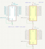
RU6: Address Decoder
This chip maps the accelerator's local SRAM and isolates it when the CPU attempts to access the video buffers on the system RAM.

DBFR_OE: This signal controls the 74245 data buffers, asserting LOW to enable the SRAM bus path.
  • Video Buffer “Hole”: The logic monitors A23-A15 and FC0/FC1 to detect the address range of the Mac Plus video buffer (the top 32KB of the first 4MB space).
  • RAM Routing: When access is detected within the $3F8000 - $3FFFFF range, the SRAM buffers are disabled and access is routed back to the main accelerator logic to handle the motherboard RAM. It also ignores Function Codes associated with interrupts or non-standard states to keep the bus clean.
RU7: Byte Lane Selection
RU7 maps the 32-bit bus to four 8-bit SRAM banks (/BYTE1 through /BYTE4). It follows the 68030 transfer bus sizing standard, using SIZ0/SIZ1 and A0/A1 to enable the correct byte lanes for aligned or unaligned transfers.

RU8: The State Machine (Timing Core)
This is the heartbeat of the memory controller and, as expected, is a much simpler state machine than the original DRAM controller. It is configured as a Registered PLD to handle timing and asynchronous handshaking via DSACK signals.
  • Wait States: It reads two jumper inputs (WS1, WS2) to allow configuration of 0, 1, or 2 Wait States.
  • Delay Logic: It uses internal registered feedback nodes (rf17 -> rf16 -> rf15) to create a shift-register style delay triggered when /SELECT goes low.
  • 0WAIT Performance: I have 45ns SRAM ICs (CY62158H) on hand, so 0-WAIT should be achievable with a 16MHz clock. For a 32-bit port, the 68030 requires both DSACK0 and DSACK1 to be asserted; RU8 drives both pins low simultaneously.
  • Write Enable: It generates /SRAM_WE only when RW is low, AS is active, and the block is selected.
Note on Clock Sync: In theory, using a 7ns GAL, the logic could generate a 31.33MHz clock using the system oscillator (15.6672 Mhz) as a source. The logic for these "budget" type accelerator boards requires the host system clock and the accelerator clock to be perfectly aligned and synchronized. Any time drift between the two will simply not work!. RU8 is intended to act as a "two-stage frequency multiplier."

Is there a better way to obtain this synchronized 31.33MHz signal, or does this "GAL-frequency multiplier" approach seem feasible? How about a PLL-based Clock Generator?

I have attached the full schematics and EQN files below. Any feedback, tips, or "gotchas" are more than welcome before I order the first PCB prototype!
 

Attachments

Last edited:
I am *super* interested in this for my Mac Plus. getting an 030 *and* the extended memory for swap into this machine, alongside the ROMinator and BlueSCSI v2 WiFi, would be a dream come true! let me know how I can contribute (pre-order, patreon, testing, etc) so this can be realized by the community-at-large.
 
I really appreciate your enthusiasm! However, it’s still a bit too early to think about testing or pre-assembled kits. I haven't seriously considered what I’ll do once the project is finished, though I will likely just publish everything on my GitHub page.

To be honest, I’m doing this mostly for the fun of it—there’s something strangely entertaining about smashing my head against a wall to make my 512Ke a bit more usable!

I am currently diving into schematics and defining an achievable scope for my skill level. My goal is to create an accelerator primarily for early Macs (128K/512K/Plus) based on the simple and clean MM Performer logic, but with several added features and improvements. I’m still at the beginning of the learning curve regarding 68030 architecture, but I feel like I’m making steady progress.

Planned Specifications:

4MB Fast SRAM (32-bit)

SCSI I/O for the Mac 128K/512K

ROM-inator support (using its own socketed PLCC ROM ICs)

Selectable 15.67 / 31.33 MHz clock speed

That’s the core of it. I believe this would be a solid open-source solution. I’m not pursuing absolute maximum performance; adding features like a 64KB cache or extending RAM beyond 4MB introduces a level of complexity that isn't achievable while maintaining the original MM Performer logic.

While I will keep the PDS connector for the SE, there are already sophisticated accelerator clones available for that model. My primary goal is to create a 'vintage solution' for early Macs that is considerably faster than what is available today.

SRAM is the smart choice here; it's reasonably affordable and eliminates the hassle of refresh logic. The SCSI I/O is already rock-solid (based on the Mac Plus logic), and the ROM-inator implementation is working well.

I am still pondering the requirements for doubling the clock speed and whether the Performer logic can handle it. Beyond faster PLDs, it will surely require buffering the address bus. I’ve noticed the Gemini Ultra/Integra and Extreme Vandal accelerators use 74ACT541s for address buffering, which seems like the obvious choice as it doesn't appear to require extra logic beyond the CPU clock. I expect the R/W signal will also need buffering for the motherboard side. To handle the clocking, I plan to use a modern multiplier like the ICS 501 or 511.

Regarding the TS Mercury DRAM expansion: I believe that design pushed the absolute limit of what was possible without buffers, even at 16 MHz. My first prototype using DRAM has been unstable due to thermal drift. While I haven’t acquired a high-quality logic analyzer yet, I suspect the issue is a combination of limited driving capabilities on the RAM ICs and poorly matched bus traces. Between that and the ROMs/SCSI, the bus is simply being overloaded. Switching to a buffered design and SRAM should overcome these hurdles!
 
In case you didn't know - the MC68030UM has a section "12.5 Static RAM memory Banks" that can be interesting for this use case. Also, manufacturers of cache tag SRAMs had application notes with detailed timing requirements for higher-speed MC68030 (some links here). A SRAM memory bank is just a SRAM cache that never misses, so some of the analysis might be relevant.
 
In case you didn't know - the MC68030UM has a section "12.5 Static RAM memory Banks" that can be interesting for this use case. Also, manufacturers of cache tag SRAMs had application notes with detailed timing requirements for higher-speed MC68030 (some links here). A SRAM memory bank is just a SRAM cache that never misses, so some of the analysis might be relevant.
Hi there!

Thank you for the heads-up! I’ve actually been re-reading Section 12.5 of the MC68030 User’s Manual quite a bit lately.

The link you provided doesn't work. I guess it's because it points to a private direct message?

The trade-off between clock frequency and bus cycles is the defining factor here. Even by doubling the clock to 31.33 MHz—while keeping the RAM access in asynchronous mode (minimum 3 cycles, DSACKx terminated) and potentially adding one or two wait states—the result still provides the most significant performance boost for the Performer accelerator.

Essentially, the raw throughput of the higher clock frequency outweighs the penalty of the extra cycles required for memory access. This is particularly true for the 68030 architecture (with its internal Harvard design) compared to the 68020 and 68000, as the '030's split caches allow it to better mask external bus latency. I guess this is the reason why we see so many 68000/68020 accelerator boards with cache.

The bottleneck for a synchronous 31.33 MHz design is the SRAM itself; I would need 4MB of 5V-parallel -SRAM type with an access time of roughly 20ns to satisfy the two-cycle window. The highest density available for such fast chips is 512Kb x 8 (4Mbit), which would require populating eight 36-pin SOJ ICs on the board to reach 4MB!. Instead, I’ve opted to maintain the asynchronous access mode—similar to the DRAM expansion board for the TS Mercury—to use the 45ns CY62158H. These offer the highest density currently in production (1Mb x 8), allowing me to populate the full 32-bit bus with just four ICs.

In theory, these 5V 45ns parts are a perfect match for a 31.33 MHz asynchronous design. I am taking the precaution of adding logic to selectively implement between 1 and 3 wait states. At 31.33 MHz, at least one wait state would be always needed.

As you can see, the SRAM is not what is holding up the Gerber files.

I am still a bit hesitant about doubling the clock speed. I am trying to determine whether, at least in theory, the Performer's core logic will remain stable if I double the frequency to 31.33 MHz using a PLL clock multiplier while adding 74ACT541 address buffers.
 
Last edited:
The link you provided doesn't work. I guess it's because it points to a private direct message?

Oups, sorry

http://www.bitsavers.org/components/idt/_dataBooks/1991_IDT_SRAM_Databook.pdf
http://www.bitsavers.org/components/ti/_dataBooks/1990_TI_Cache_Memory_Management_Data_Book.pdf
Enhancing MC68030 performance using the SN74ACT2155 cache.

while keeping the RAM access in asynchronous mode

It might be easier to use synchronous mode on the '030n actually, as you don't need bus sizing.

The bottleneck for a synchronous 31.33 MHz design is the SRAM itself; I would need 4MB of 5V-parallel -SRAM type with an access time of roughly 20ns to satisfy the two-cycle window

3-cycles synchronous might be easier to implement than 3-cycles async; and if you need more than one bank of chips for the chosen size, you can have two banks and get 3-1-2-1 burst reasonably easily (maybe 3-1-1-1 with fast enough SRAM).
 
You’re correct that 32-bit RAM avoids bus sizing, but the 68030 still has to interface with 68000-era legacy hardware. That is precisely why the bus sizing feature exists in the first place. Modifying the core logic to handle the handover between Fast and slow RAM for video buffer access—specifically switching from a 2-cycle synchronous to a 3-cycle asynchronous mode—would be a massive undertaking.

Right now, the accelerator toggles RAM access by sniffing the memory address space (handled by PLD RU6), while the main state machine manages the arbitration and asynchronous signal translation. Re-engineering that logic is definitely beyond my current reach! Furthermore, adding the logic required to handle an external cache, which would effectively require scrapping and replacing the current design, is a challenge well above my skill level. So, asynchronous mode for SRAM in this context is not just an option; it is simply mandatory.
 
Last edited:
An update:

I’m evolving my design to use latched buffers for both the address (74574s) and data (74646s) buses. If you look at more advanced 68030 accelerator boards you will notice immediately that they all use latched buffers.

These provide at least two absolutely necessary requirements for increasing the clock speed of the Performer:

Isolation: They "hide" the daughterboard's local traffic (such as the CPU talking to its own Fast RAM) from the host system. The original Macintosh Plus/512 was designed for an 8 MHz clock; when you hammer those old traces with faster bus signals, the capacitive load increases significantly, degrading the signal integrity. Because those boards were never designed for such speeds, the resulting impedances are often far out of spec.

Stability: The latches "freeze" the bus state for the Macintosh Plus/SE motherboard for the exact duration its own asynchronous cycle requires.

The crashes I’ve been seeing in my DRAM prototype are likely direct results of these integrity issues, stemming from long traces with poor impedance matching.


This approach is modeled after the design seen on the Gemini Ultra and Vandal accelerators (an educated guess made after carefully studying photos of them online). While I could use 74646s for both buses, using the 74574 for the address bus saves much-needed space, allowing for a more compact layout and a reduced PCB footprint.

I am still polishing the logic that will control these latched buffers. So far, the project seems attainable because I am not attempting to dive into synchronous cycles. That would require far more complex logic that is currently beyond my experience level (keeping it asynchronous is a much more manageable path for this accelerator design).

As an interesting note, the DRAM expansion board of the Mercury 030 uses 74245 data buffers to drive the RAM ICs, rather than the host system data bus. I see this as a limitation for any clock speed increase. I am attempting to flip the logic to use the buffers (latched type) on the host side. The CPU load will be limited to the local logic and the SRAM ICs. That seems to be a much more common arrangement in high-profile 68030 accelerators.

While this level of "over-engineering" might seem like overkill for a board without a cache and limited to 4MB of RAM, it ensures signal integrity is strong enough to safely double the clock speed to 31.33 MHz.

From what I’ve learned so far, the host system and accelerator clocks in the MicroMac Performer’s core logic are not uncoupled; they remain synchronized in phase. This makes the logic far simpler than that of more sophisticated 68030 accelerators. However, I’m hopeful that by introducing these bus-driving improvements, the core logic will perform reliably at double its default speed using a PLL clock multiplier. Any feedback or back-and-forth comments are more than welcome!
 
Last edited:
It’s been a while since my last project update.

A lot has happened since then, and I thought it might be entertaining; and helpful for me, to share my progress with you all.

Along with other new features I’ve been exploring for a beefed-up version of the Mercury board (like extended RAM), I’ve been scouring for any design information regarding the buffered buses used in high-end 68030 accelerators like the GEMINI line, but there is virtually none. I wonder if I’m just looking in the wrong places?

Anyway, I haven't ordered a second PCB run yet; I’m still tinkering with the first prototype, learning more about the 68030 architecture and the digital design challenges of the 90s. I must confess, it has captured my attention; it’s a rewarding feeling to know that I am slowly but steadily learning something completely new, and I’m still thoroughly entertained.

As I mentioned in earlier posts, the DRAM controller is finally "mostly" working after I tracked down a missing connection on the DSACK1 trace and resolved the state machine interlock between the RU8 and RU9 PLDs using opposite-phase clocks (many thanks again to JC8080 for the help with those clock phases!).

I’ve also been obsessively (and forcibly for exploring how to introduce an extended RAM bank) unraveling the logic implemented in the TS Mercury’s DRAM controller. I won't bore everyone with the technical details, but if anyone wants to delve into how it works, feel free to PM me; the way the CBR refresh logic is implemented is incredibly complex but fascinating.

For a while, I was convinced that simply switching to SRAM would improve the overall stability of the TS Mercury design and allow me to start tinkering with higher clock speeds, creating more wait states for the fast RAM controller, etc. That is likely true, as the DRAM ICs I chose are incredibly finicky. But, as in life, that is not the whole story!

I’ve noticed that many 72-pin SIMMs from the 90s using these chips include Schmitt-trigger buffers with built-in termination for MA signals (such as the 74FCT162244).

The original TS Mercury DRAM board lacks any kind of termination for the 74257 outputs or the CAS signals. That made sense in the original design: each SIMM contained eight chips, providing enough capacitive load to absorb any noticeable ringing on the MA and CAS lines at 16 MHz. In that scenario, adding series resistors would have only introduced unwanted skew on an already tight timing budget.

As for high-end accelerator designs, it seems all of them introduce series resistors to the MA and control signal lines, allowing for the use of faster PLDs.

To make matters worse, since I am using high-density DRAM directly soldered to the PCB (only two chips), the overall capacitive load is much lower, making ringing a significant factor to consider if I intend to use faster PLDs and buffers with higher clock speeds.

On the first PCB prototype, the DRAM chip that has no buffers (D15–D0) is incredibly far from the CPU, with long traces (averaging 30 cm in length), a width of 15 mil, and many vias along the path.

No wonder the board warms up and crashes!

However, adding transparent buffers and termination, along with shorter and thicker traces, doesn't solve the core issue with this budget DRAM controller design. Don’t get me wrong; the design is clever and delivers, given that this is the most basic design offered in the TS accelerator line, but it is operating at its "reliability limit."

This bus control design barely holds up for a 16 MHz CPU clock. An important chunk of the timing budget is being consumed by the skew introduced by keeping the host address and data buses driven during fast RAM accesses.

I am considering adding a PLL clock multiplier to derive a 3X or 4X clock for the accelerator from the 8 MHz reference. But before I even start tinkering with higher clock speeds, I have to address the problem of not having isolated or "frozen" host buses during fast RAM accesses.

The TS Mercury DRAM controller arbitration method for the shared data bus is quite simple: when a host address is hit (RU6 PLD), the buffers are disabled (isolating the fast RAM data path), leaving the 68030 to interact with the host.

This has a significant handicap: when the 74245 buffers are active (the fast RAM data path is open), the host's data bus remains unnecessarily driven. The resultant skew (mostly during write cycles) of this load becomes critical for clocks beyond 16 MHz.

Regarding the host address bus, it is permanently driven by design, whether or not the DRAM controller is installed. While direct driving was common in 68000-based architectures, it is highly unusual for the 68030 and effectively pushes the 16 MHz 68030 to its limit.

Even the earliest 68030-based computers from Apple and Commodore employed some form of address bus buffering or management to handle increased loads at clock speeds not seen in most 68000-era devices.

I should emphasize that all of this is still very new to me; I am an EE who has spent most of my career in completely unrelated fields, and I am learning as I go. That said, in my humble opinion, the fact that the TS engineers achieved stability at 16 MHz with the fast RAM board installed is remarkable; they pushed the CPU’s drive capabilities to their absolute limit in the Mercury design.

By using 74245s with built-in termination for the A-side and high-current Schmitt-trigger drivers on the B-side, signal integrity can be guaranteed toward the DRAM ICs, but it does not address the permanent drive of the host side during fast RAM accesses.

So, I’ve been trying to understand how more advanced accelerator boards with higher speeds tackle this issue. The answer seems as straightforward as anyone from this EE field would see just by looking at those boards. Unlike the Mercury design, what they do is "freeze" the host buses during fast RAM accesses.

Practically all of them use the same approach by interposing bidirectional registered transceivers (74646s) for the data bus and latched buffers (74574s) for the address bus. (In higher-end accelerators like the Gemini Ultra/Integra or the Vandal Extreme, which work with clocks up to 50 MHz, a CPLD like the Xilinx 2018 is used instead of 74646s to arbitrate the data bus.)

So the question is: what logic do I need to control them and make them perform on the Mercury board? That’s where I am right now.

You would not believe how scarce the information is regarding this aspect; I haven’t been able to find any textbooks or tech docs explaining this, nor any examples of the underlying logic.

As I understand it, those GEMINI models use a type of PLD that no one has been able to "hack" (the GAL22V10) to extract the JEDEC files. The same thing happens with the Xilinx CPLDs. Consequently, no one has ever taken the effort to reverse-engineer a schematic from them.

So, here is the challenge: I have to create my own logic control solution for these registered buffers, based on what I have learned while delving into the 68030 accelerator designs.

I have developed a custom logic control solution for these registered buffers based on what I’ve learned while delving into the 68030 architecture.

The design seems sound on paper, but I’d like to share it and request feedback from anyone familiar with the theory behind these accelerator designs. I am specifically looking for any potential flaws in my custom logic for these “bus freezers.”

I believe providing a snapshot of the schematic should be sufficient for those with a trained eye for these matters.

ADDRESS BUFFERS

74574s.png

Let’s start with the address bus, as it seems the CP logic could be implemented easily.

The CP input is an active-high signal.

HOST_ADDR is also an active-high signal and is already generated by the baseline logic of the DRAM controller at RU6. It is the same signal that controls the 74245 buffers on the original design, and its function is to flag (HIGH) any address or CPU state that does not belong to the fast DRAM address space.

No race conditions should arise here by using AS_30 as a gate to the host address bus, since there is another AS (AS_00) synthesized by the accelerator’s baseline logic that is synchronized with the host clock (8 MHz).

Therefore, the propagation delay involved in synthesizing and aligning AS_00 to the host clock guarantees that the address bus is fully stable before AS_00 drops.

DATA BUFFERS

74646.png

During 68030 CPU read/write operations, the host data bus must be isolated for access cycles that fall outside the host memory map.

The isolation part seems straightforward by controlling the /G pin like this:

/HOST_DBFR_EN = HOST_ADDR * /AS_00

Again, HOST_ADDR validates that the address belongs to the host memory map. AS_00 will frame the enabling window of the buffer to 68000 device access cycles, tri-stating the A-side of the buffer once the 68000 host cycle ends.

I am configuring the 74646s to make the transceivers transparent for read cycles. The reason is that, in principle, I should not have concerns when the host is driving the data bus, as there is plenty of timing budget within a host cycle (8 MHz) to get the data stabilized before the synthesized LDS/UDS strobes get asserted. The fastest and most critical device on the host side would be the onboard RAM, and the Mac 128/512K already have 74244 output buffers to drive the data bus in read operations.

For a host access, the data must be latched as soon as it is fully stable on the 68030 bus side and held on the A-side until the write operation ends.

The 74646 is perfectly suited for this role, which explains why it is so commonly used in earlier Novy / Gemini accelerators.

With SBA tied to GND (enabling the registered path from B to A), CPBA must transition from L to H as soon as the data is stable on the B-side (the 68030 bus).

On the rising edge of CPBA, the data is stored in the B register and refreshed on the next rising edge.

Because SBA is tied to GND, the data in the B register is driven in real-time on the A-side (host) and held.

Following the asynchronous protocol of the 68000 architecture, synthesized LDS/UDS strobes by the baseline logic from the accelerator will then assert, instructing the targeted 68000-based device to latch the data from the host bus (A). Finally, when the DTACK assertion is received by the accelerator’s baseline logic, it is translated into DSACK1 (PLD U4), effectively ending the cycle.

So CPBA must flip from LOW to HIGH only once the data is ready on the 68030 bus.

The proposed equation for CPBA is:

DBFR_BA.PULSE = ADDR_HOST * /AS_30 * /DS_30

I could just use DS_30, but apparently, this makes the strobe less prone to glitches for a reason I don’t fully understand yet.

Apparently, the logic of accelerator boards like the GEMINI doesn't use /DS_30 for anything, and I suspect they use /AS_00 in the buffer logic control instead.

But I don’t know the timing relationship between DS_30 and the synthesized AS_00 in the logic of the Mercury board.

It could very well be possible that the delay due to clock alignment are enough to guarantee AS_00 is always asserted after DS_30; that could explain why DS_30 is apparently not used for anything regarding the buffer control on those high-end accelerator boards.

Also, the time delay due to clock alignment widens between DS_30 and AS_00 as the accelerator clock speed (frequency) is increased.

So if the previous holds, CPBA could just be:

DBFR_BA.PULSE = HOST_ADDR * /AS_00

And this is a dilemma. The extra PLD I am adding to the logic is falling short of one feedback pin. If I could forgo DS_30, then just one extra PLD will be enough for the new buffer logic control and SCSI control signals. But how to be sure? I could use the oscilloscope and find out, but I would like to deduce it by just analyzing the logic.

So, during every rising edge of this signal, the data on the B side latched and driven on the A side. When the access cycle ends, /G will disable the buffers.

Well, that’s it for what it's worth regarding the buffers.
 

Attachments

  • 74574s.png
    74574s.png
    336 KB · Views: 0
Last edited:
Back
Top