A few months ago, I worked out how to run 48MB in a PowerBook 500 Series. Inspiration was taken from Toyoki's 64MB mod for PPC upgraded 500-Series notebooks. The concept is similar – tap into unused RAS lines on the memory controller to bump maximum RAM above 36MB.
You will need:
Here's my RAM card with 6 of the 8 new chips soldered down, and a 7th in position. You can hardly tell they are stacked. Note the two lifted pins per chip.
Here's a side view of the stacked chips soldered down.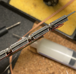
Use repair wire to connect up the RAS pins across the four chips at the top, and another repair wire to connect up the other four chips at the bottom. Don't connect them together! Run two trailing wires (one from each bank) to the RAM card connector. I left the NC pins floating/disconnected.
Pins 28, 29 and 30 are labelled 'reserved' (more on this in a bit) in the Dev Note, page 35. I used pins 28 and 30 to send my RAS signals back to the CPU card, as shown:
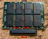
That's your RAM card done.
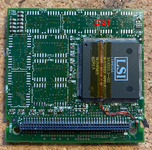
Now, take your CPU card, remove the onboard RAM, and run two repair wires as shown to pins 190 and 191 of the Pratt MemIC. Make a cut on the trace leading out from pin 190/RAS0.
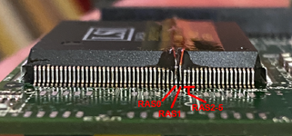
Side view of RAS0 (Pin 190) and RAS1 (Pin 191), showing repair wires soldered on. Definitely a fiddly job.
Moving to the RAM card connector on the top side of the CPU card, we need to peel back the serial# sticker and cut the traces leading to Pins 28 and 30 as shown.
These go back to unknown pins on the Pratt MemIC, but aren't needed. @demik theorised they could have been used during development for ROM cards.
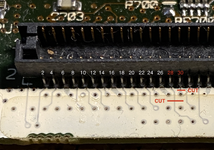
Finish by running your repair wires up to the pins.
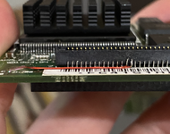
Assemble your machine, and there you go – 48MB in a PowerBook 500 Series.
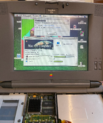
This was one heck of a difficult mod to do, it took me two attempts! Worth it though. I'm hoping to eventually create a 500 Series 'Reloaded' CPU card with 16MB onboard and programmable oscillator, if there's enough interest.
So, how many RAS lines are unused? Let's look at the Dev Note:
Armed with this information, we have a strong basis for a successful mod. Now, over to the practical side.
That's six in total. RAS 2-5 go to the RAM connector, RAS 0 is connected to the single 4MB bank on the CPU card itself, and RAS 1 is not used. Each RAS line corresponds to one bank of up to 8MB, so a theoretic total of 48MB is possible. This is backed up by the Dev Note, which says:DRAM_RAS_L[2–5] Row address select signals for up to four banks of DRAM. (The first two banks, selected by DRAM_RAS_L[1:0], reside on the CPU and memory module.)
@joevt also looked at the Universal Tables in ROM and saw that 6 banks of 8M are supported.The RAM array is located in the system memory map between addresses $0000 0000 and $02FF FFFF
Armed with this information, we have a strong basis for a successful mod. Now, over to the practical side.
You will need:
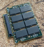
- A 32MB RAM expansion card like the one in the following photos
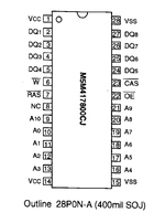
- 8x 2MB 28-pin TSOP (thin profile) chips
- Repair wire
- Patience, decent eyesight and a steady hand
- RAM Card
- Convert a 32MB RAM card to 48MB by stacking chips
- Run wires from the /RAS pin of the new banks to unused pins on the RAM card connector
- CPU Card
- Desolder the onboard RAM.
- Cut 3 traces
- Run wires from RAS0+1 to unused pins on the RAM card connector

Here's my RAM card with 6 of the 8 new chips soldered down, and a 7th in position. You can hardly tell they are stacked. Note the two lifted pins per chip.

Here's a side view of the stacked chips soldered down.

Use repair wire to connect up the RAS pins across the four chips at the top, and another repair wire to connect up the other four chips at the bottom. Don't connect them together! Run two trailing wires (one from each bank) to the RAM card connector. I left the NC pins floating/disconnected.
Pins 28, 29 and 30 are labelled 'reserved' (more on this in a bit) in the Dev Note, page 35. I used pins 28 and 30 to send my RAS signals back to the CPU card, as shown:

That's your RAM card done.
Now, take your CPU card, remove the onboard RAM, and run two repair wires as shown to pins 190 and 191 of the Pratt MemIC. Make a cut on the trace leading out from pin 190/RAS0.

Side view of RAS0 (Pin 190) and RAS1 (Pin 191), showing repair wires soldered on. Definitely a fiddly job.

Moving to the RAM card connector on the top side of the CPU card, we need to peel back the serial# sticker and cut the traces leading to Pins 28 and 30 as shown.
These go back to unknown pins on the Pratt MemIC, but aren't needed. @demik theorised they could have been used during development for ROM cards.

Finish by running your repair wires up to the pins.

Assemble your machine, and there you go – 48MB in a PowerBook 500 Series.

This was one heck of a difficult mod to do, it took me two attempts! Worth it though. I'm hoping to eventually create a 500 Series 'Reloaded' CPU card with 16MB onboard and programmable oscillator, if there's enough interest.
Last edited:


