• Updated 2023-07-12: Hello, Guest! Welcome back, and be sure to check out this follow-up post about our outage a week or so ago.

SE/30 advice needed regarding previous repair

croissantking

Well-known member
I picked up an SE/30 on eBay in very good condition. It runs however there are some odd issues so I’ve been inspecting the logic board. Someone has had a go at recapping it but they have done a bodge job (it’s terrible) and even ripped some traces in the process, so I am redoing the work.

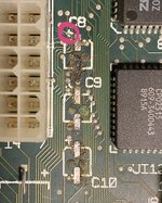
Regarding the attached image, there is a ripped trace and I assume that the repair wire (neatly installed, surprisingly) is in place for this reason. Can someone who has some knowledge of this board please advise if this repair has been done correctly?
B6350DAD-D90C-4126-BEB9-8ACE4305AEA6.jpeg
 
Last edited:

Byrd

Well-known member
Someone slipped a screwdriver on their SE/30 by the looks of things - the repair does look a little rough.

Usually the standard is to gently scrape back either side of the disconnected wire, flux/reflow and run the bodge wire between, cover with clear nail polish to protect. PS. The blue bodge wire is a factory patch
 

Bolle

Well-known member
Factory patch wire indeed. Leave it alone. The cut trace is also from the factory. All early boards have that wire+cut.
 

Byrd

Well-known member
Something new learnt today - had no idea the notch taken out was factory. Imagine that was your job at Apple "yeh Barry is gonna do the wire you can grab a chisel and knock out this trace"
 

croissantking

Well-known member
Wow, I would never have thought that the notch would have been a factory modification. That’s very interesting.

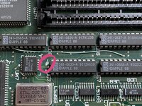
The only area that I now need to turn my attention to is here, in this attached image. One of the capacitor solder pads is ripped off so I assume I’ll need to tap into the VIA next to it using a short repair wire. Also, the area circled in pink has exposed traces and one of them doesn’t show continuity with a multimeter. So imagine I’ll have to use a bodge wire to link up the two VIAs at either end. I can see that it would be hard to do surface mount soldering next to a large connector and this is probably the reason the previous owner messed up.

49859EE9-4D8E-4321-9424-F1B2E6D47CAA.jpeg
 

croissantking

Well-known member
Let me know if you have any tips for my upcoming repair work! I am waiting for the capacitors and 30AWG 'Kynar' repair wire to arrive.
 

drmadison

Member
As someone who recently did a recapping on his own SE/30...

Try to clean up all that gunk as much as possible where the old caps were.

Go slow and be patient, especially if you got the same "replacement" caps as I did, as they're larger than the old electrolytics and so there's very little pad-space available.

Extra careful around the plastic connector in that picture - I ever so slightly warped mine just by barely bumping it with my iron - thankfully I noticed immediately and it didn't warp so badly that I can't plug the analog board in.

In my own de-capping, I lifted 2 of the pads (I know, bad me! I should've ordered an hot air gun to do a cleaner job and not tried to do it just with a soldering iron...) and wasn't able to bodge to the vias. I tried scrapping them off a bit but maybe I was just too gentle, I was worried about damaging them further so instead I bodged to pins on whatever chip the line eventually went to instead. So... expect to either use more force than I was willing to if you want to bodge to vias, or just follow all the way :)
 

croissantking

Well-known member
As someone who recently did a recapping on his own SE/30...

Try to clean up all that gunk as much as possible where the old caps were.

Go slow and be patient, especially if you got the same "replacement" caps as I did, as they're larger than the old electrolytics and so there's very little pad-space available.

Extra careful around the plastic connector in that picture - I ever so slightly warped mine just by barely bumping it with my iron - thankfully I noticed immediately and it didn't warp so badly that I can't plug the analog board in.

In my own de-capping, I lifted 2 of the pads (I know, bad me! I should've ordered an hot air gun to do a cleaner job and not tried to do it just with a soldering iron...) and wasn't able to bodge to the vias. I tried scrapping them off a bit but maybe I was just too gentle, I was worried about damaging them further so instead I bodged to pins on whatever chip the line eventually went to instead. So... expect to either use more force than I was willing to if you want to bodge to vias, or just follow all the way :)
Believe it or not, my photo is after I already cleaned up the board with 50% IPA and a toothbrush– I think the gunk you see is the original solder mask that's been burned/melted (but I'm willing to be corrected if that's not the case).

I had good results with the 'twist and pull' method of removing the caps. I practiced on a dead G3 motherboard first. The one ripped pad you see was already missing.

I've desoldered the vias I need to jump, it should now be straightforward to stick a repair wire through the board and resolder.

I've ordered the same type of electrolytic caps as the originals, although I know that a lot of people are using tantalum caps now.

Working around the plastic power connector looks like a PITA!
 

Aeroform

Well-known member
I'm really no expert compared to others here, but will offer my tips anyhow. Do with them what you please 😂

For the cut traces by C8 I would simply scrape of some of the solder mask on either side (about 2mm), put on some fresh solder and run a super short bodge between. No need to run the full distance between two VIAs.

For cleaning up the pads and area around, I'd use some flux, add fresh solder and then gently rub / remove the solder & gunk with a desoldering braid. Also 99% IPA I'd guess is better than 50%. I've also had some luck with a mixture of baking soda & vinegar followed by IPA. Now to me it does look pretty burnt, like whoever did that "repair" had their iron turned up too high.

I great tip I've learned from building drones and soldering plastic connectors would be to keep it plugged when you work around it. That way, if it warps/melts due to heat, it would hopefully still keep the shape enough to not hinder plugging in/out. If I'm not completely mistaken I believe you can disconnect the cable from the A/B board side which would let you keep it plugged on the MB when working on it. Now that does add the chance of you melting the cable instead I guess haha..
 

timtiger

Well-known member
For cleaning up the pads and area around, I'd use some flux, add fresh solder and then gently rub / remove the solder & gunk with a desoldering braid. Also 99% IPA I'd guess is better than 50%.
I do it the same way: Gently rubbing the pads/gunk with lots (!) of flux and desoldering braid. Be careful and do not overheat pads and surrounding areas…

After cleaning the board this way, I use little ipa (99%) and a special electronic cleaner to minimize corrosion effects.
 

cheesestraws

Well-known member
I great tip I've learned from building drones and soldering plastic connectors would be to keep it plugged when you work around it. That way, if it warps/melts due to heat, it would hopefully still keep the shape enough to not hinder plugging in/out. If I'm not completely mistaken I believe you can disconnect the cable from the A/B board side which would let you keep it plugged on the MB when working on it.

That is a sensible tip. Note, though, that the power connector is a part you can still get, and there are people selling perfectly adequate "clones" on eBay for cheap also. So if you knacker the plastic of the power connector, it will be annoying but not much more than annoying: you can get a replacement fairly straightforwardly.

For cleaning up the pads and area around, I'd use some flux, add fresh solder and then gently rub / remove the solder & gunk with a desoldering braid.

Yes, this is what I do too, with the emphasis on gently. Personally I always try to stroke the braid from the track end of the pad to the "free" end of the pad to try to avoid lifting it, but this may just be superstition.

Also 99% IPA I'd guess is better than 50%.
After cleaning the board this way, I use little ipa (99%) and a special electronic cleaner to minimize corrosion effects.

A tip here is that if you wash with 99% IPA after any water-based cleaners, the IPA will help chase the water out of corners. It breaks down the surface tension of the water so it's easier for it to run off, and the mixture of water and IPA also (up to a certain point) is easier to evaporate off than just water on its own. So your board will dry quicker, and it's less likely you'll end up with hidden pockets of water.
 

Jamieson

Well-known member
Yup agreed, in the first pic that trace was cut deliberately. The blast point is too accurate. Only imperial technicians are so precise.
 
Top