• Updated 2023-07-12: Hello, Guest! Welcome back, and be sure to check out this follow-up post about our outage a week or so ago.

HD20 Schematics required

trag

Well-known member
Is there an Apple II Disk Controller card which does the same thing as the IWM? I ask, because I have one in a box around here somewhere, and it's built out of discreet components. It should be possible to reverse engineer the IWM from that, if it has the equivalent of an IWM on board -- unless, of course, there are unreadable PALs involved.

I love the work you guys are doing.


Dennis Nedry

Well-known member
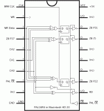
I've never done anything with PALs before, nor have I ever really known much about them, but something that puzzles me about this PAL is that all of the unused outputs, latched or not, change states. This seems like potential evidence that those outputs are used internally as previous states for the next clock cycle, for state machines.

Seeing this in graphical form makes me think that input 1 (WR) may have something to do with the 3-state of the asynchronous I/O (RD). RD can also be used as an input when it's high-impedance, and I certainly didn't test for that.

If I had some resistors handy, I'd run it once with a pull-up and once with a pull-down on the RD pin. Any difference would indicate high-impedance. Any differences in other outputs when the RD output is different would indicate that it is being used as in input during its high-impedance state.

unless, of course, there are unreadable PALs involved.
All PALs are completely readable with enough persistence functionality-wise, they are finite state machines! }:) It's just tempting to see a pattern and assume that's it before every possible combination is exhausted. I bet this PAL is still directly dumpable, it's from 1985. I don't have anything that can do that for me though.

PAL.gif


Dennis Nedry

Well-known member
I found a 10k resistor and ran the test. It turns out that high-impedance state depends on OE. Well, I guess that makes sense. It still doesn't make WR do anything. Within the scope of the original test, I have verified that this I/O does not function as a meaningful input during high impedance state.

To do this, I ran the test once with the I/O pin pulled up and once with it pulled down. I then compared the outputs of the 2 tests. Only the I/O pin was not the same between the 2 tests, it didn't affect any other outputs. The ones that were different show us high-impedance state.

It is possible that there was an extra input pin and they went ahead and ran a WR trace to it in case they might need it - then they could just replace the PAL if they need WR in the logic. That seems reasonable.

PAL.gif


Dennis Nedry

Well-known member
As I go back over my work, I think I may have made some critical errors ...

I believe that I got confused 2 ways: flip inputs 0 - 7 to 7 - 0, and counting 0-based vs. 1-based. I'll go through it more much more carefully now and redraw the chip again.


Dennis Nedry

Well-known member
The diagrams I provided are almost completely wrong, I don't really know what happened. But this data is well-verified this time.

Here is the key:

Output:

F0 = Pin 12: RD

F1 = Pin 13: Z8 P22

F2 = Pin 14: nc

F3 = Pin 15: nc

F4 = Pin 16: nc

F5 = Pin 17: Z8 ?

F6 = Pin 18: Z8 P31

F7 = Pin 19: nc

Input:

A = Pin 9: nc (notably missing from minimized logic!)

B = Pin 8: PAL OE'

C = Pin 7: CA0

D = Pin 6: CA1

E = Pin 5: CA2

F = Pin 4: Z8 P37

G = Pin 3: WR Data

H = Pin 2: WR

Logic Friday Minimized:

F0 = C' E + D E + D F + D' E' F' H' + D' E' G H;

F1 = E + C' D ;

F2 = F + G' H + G H';

F3 = F + G' H';

F4 = G H + F' H';

F5 = C + D + E' ;

F6 = C' D' E' ;

F7 = G H + G' H';

3-state output is still based on OE' for F0 (Pin 12), and this was figured in to the source data by entering don't cares for this output when it is in 3-state mode. Unless there's hidden logic on previous states, for example, using the latched data stored in F2, F3, F4, I'm confident that this is the correct solution to the PAL chip now.

It honestly terrifies me that F2, F3, and F4 are not =1 or =0. And the complexity of F0. It could be that F0 is a function of F2, F3 and F4, which would indicate a state machine that I haven't found yet. I'm not worried about F7 because it's not latched.


Gorgonops

Moderator
Staff member
It might be possible to figure out what the Z8 is doing on the IWM side and somehow separate that from what it is doing on the Rodime side...
Separation is good, since of course for the purposes of replicating the functionality of the HD-20 with modern components any details of the Rodime drive itself are not very important... although you do need to understand enough to know what sort of commands get sent to it. The Rodime drive *probably* looks basically like an ST-412-style drive, in the sense that it takes/produces a serialized data stream and uses separate control lines to do things like track stepping/head selection/etc. An "intelligent" flash-based (CompactFlash, SD card, etc) replacement is probably going to support simple LBA addressing, where you can treat the drive as a block of sectors numbered from zero to XXXX. What you need to know regarding the Rodime is:

A: Does the Mac send track/platter selection commands, IE, does the Mac know the "geometry" of the HD-20, or is it treated linearly and the Z8 takes care of the the 3D translation? (Or, possibly, does the controller chip on the Rodime drive itself handle that, and it presents itself to the IWM board as linear?) I *thought* at some point we'd found some documentation saying the HD-20 presents itself to the Mac as a linear device, but the problem is that, given the style of Apple documentation, that may simply mean the *driver* presents it as linear.

B: Does the Z8+IWM do any transformation of the data stream received from the Mac before it's stuffed onto the drive? One theory which *may* be reasonable: If sector data from the Mac is GCR encoded by the normal floppy routine in the .Sony driver before it's sent to the HD-20 it *may* simply be written to drive in the "nybble-ized" form received from the IWM on the other end, rather than every sector being processed by the Z8 beyond the Z8 grabbing it off the IWM bus and stuffing it at a shift register leading to the Rodime's write circuitry. (Perhaps using the onboard SRAM as a buffer to compensate for differing data rates.) GCR produces bit patterns essentially similar to MFM encoding, it may be perfectly reasonable to use the data straight from the Mac.

If "B" is true that may have implications for looking for control bytes. See below:

So the key here looks like figuring out the Z8 code. Assuming that the Z8 is ROMless and runs exclusively from the external ROM chip that I dumped, it might be possible to figure this out with that approach. I'm grateful that you explained this for me because I would have done exactly what you said - I would have started looking for patterns in decoded data coming off of the IWM, which won't work with this strange auto-checksum / encoding stuff if that's in there.
I would try looking for the translation table bytes in the ROM dump. If the Z8 is decoding/encoding GCR there should be two tables which match the .Sony driver's tables, which you have in that NetBSD source code. Translation tables supposedly lifted straight from the Apple .Sony driver are near the start of that NetBSD source code.

It is also possible, as it seemed you alluded to, that the Mac skips it's encoding / decoding process specifically when talking to an HD20, thereby not needing anything to decode it in the HD20. In this case there might be unencoded data fresh off of the IWM, but I'm not really counting on it anymore.
A case like this may be possible: You *do* need to encode according to the rules (IE, no more than two zeros in a row) to use the "data pump" on the IWM. But...

1: Sector data from the Mac is GCR, but the Z8 doesn't decode it; it just shovels it to and from the hard disk. Likewise reads just shovel bytes from the hard drive to the IWM. (Again, probably through a RAM buffer.)

2: Control signals either use a simpler encoding like FM (similar to how address marks are written on floppy disks) and thus use a different table/are calculated directly, or the IWM's serial data pump isn't used at all for "housekeeping" and control signals/sector addresses are bit-banged over the control lines.


Dennis Nedry

Well-known member
Because some unencoded Mac code is stored in the HD20's ROM, one of 2 things is probably true:

-At least some encoding occurs in the Z8

-IWM supports some sort of mode where raw data goes in at the HD 20 and comes out raw in the Mac.

How could IWM require data to be encoded if it doesn't do any encoding/decoding itself? Is it calculating checksums or something? :?:


Gorgonops

Moderator
Staff member
How could IWM require data to be encoded if it doesn't do any encoding/decoding itself? Is it calculating checksums or something? :?:
Two reasons:

1: Requirements for "you need a bit ever X nanoseconds" stem from the mechanics of floppy drive reading and writing itself. I am *not* enough of a scientist to tell you exactly why they are what they are but collectively they amount to "If you don't keep changing the state of the floppy head from zero to one and back again often enough it's not going to write recoverable data". A long string of "1s" is okay, ideal even, because it gives lots of pulses for the data separator to lock onto when it's reading it back. A long string of zeros, IE, no pulses at all, will screw you because between magnetic flux migration and the not-completely-predictable rotational speed of a floppy drive there's a good chance that you will lose track of how many zeros were supposed to be between the last "1" and the next "1".

In order to comply with that requirement you somehow have to convert bytes which contain long strings of zeros to bytes that have no more than two zeros in a row. (Originally this was specified as "more than one zero" in a row, which in its simplest form is "single-density" or "FM" encoding consisting of a clock bit and a data bit. Apple's GCR pushes it to two, which is why the Disk ][ could store 140k on a floppy in 1979 while a machine using an early Western Digital Single Density controller, like the TRS-80 Model I, only got 90k on the same disk.) The IWM does not do this itself so the CPU has to do it. Literally all the IWM does is provide the hardware for turning those encoded bytes into pulses suitable for the disk drive and recovering said pulses from the drive. For actual reading and writing it does almost nothing more than that.* (asterisk sort of important. See later.)

2: The IWM was built to do number one, so even if it's *not* in this particular application dealing with a troublesome and unreliable data stream sucked off a floppy drive its data recovery hardware is still designed to do that job, so if you try sending it an unencoded data stream with a bunch of zeros... it may choke. The data sheet talks about how the data separator semi-derives its clocking from the last bit received, and it's unclear to me if it will start screwing up if it you send it too many zeros, or if it will work fine(ish) as a UART in this one case since the clocking is going to be more predictable than a disk read and it will just happily keep shoving zeros into the output shift register however many you send. And... the next paragraph is about that asterisk.

(*) There's a head-hurty part of the IWM's data sheet where it talks about the difference between "synchronous" and "asynchronous" modes (the basic difference between those two is "synchronous" is the "slavishly emulating the Disk ][ controller" mode" and "asynchronous" is "I'm slightly smarter about not needing constant CPU attention just to shift out bits, IE, I can at least handle watching a clock input on my own". Around that part of the data sheet, notice the parts that talk about the data format consisting of an "8 bit nibble with the MSB set". In Apple's GCR encoding scheme all valid encoded bytes have a "1" as their most significant bit. (Look at the translation table in the NetBSD driver; none of the "toDisk" bytes are less than 0x80.) Apparently testing for "1" in the MSB of the disk-read shift register is how the old Apple ][ disk routines used to tell if a full byte had been read in from the disk, and the because of that the IWM's hardware has been built to treat the shifting of a 1 into that position as a special event, latching or "stalling" the shift register depending on which mode (async or sync) the IWM is running in. The implications of this aren't totally clear to me, but... it seems to me that at the very least even if it *would* reliably read a string of zeros if you fed it 8 zeros in a row (or any byte starting with "0", for that matter.) you wouldn't know from the polling loop that you'd received a whole byte unless you were keeping track of the expected time to get a full byte independently. (Because you won't get the MSB bit telling you got 8 bits, and that's the only clue the IWM gives you.)

It's... not impossible, maybe, that the software on both sides gets around this by putting the IWMs in sync mode (to avoid the latching), counts the time 8 bits would take when reading, and then grabs 8 bits off the shift register and assumes it's good. But that sounds really sketchy to me, and... there's something else that fills me with dread. It's quite notable that the "diskTo" and "toDisk" tables are different in the NetBSD IWM driver... like, completely different. (Like, diskTo is filled with values that *are* lower than 0x80) Someone needs to sit down and stare at an Apple ][ disk driver. I'm wondering if the values recovered by the IWM's data separator are inverted or something compared to the bytes written, or if there's some shift/XOR going on in the driver that explains it.

Anyway, these are at least some reasons why I'm not at all warm to the idea the IWM is acting like a non-munging UART here. But there may be some completely undocumented mode where it does.


Dennis Nedry

Well-known member
I'm sorry Gorgonops, but I just don't have an attention span long enough to read through all of that and understand what you said right now.

Here is F0 from the PAL considering 1 previous state from all other outputs, Px being the previous state of Fx:

Code:
Minimized:
F0 = B  + D F  + P2 C' F'  + D G' H' + P2 P7 D' E'  + P2 D' E' F' ;
This is from a very limited sample size so it is absolutely not conclusive in any way. Interesting that it seemed to find some connections though.

There are 32,768 possible input combinations considering 8 inputs and 7 feedback outputs (it can't really feedback itself as a previous state because it's not registered.) I tested 256 of them for this.

Come to think of it, because it's not registered, it would need the CURRENT state of the other outputs, DURRRRRR

So this test is rubbish.

edit

;D with current states

Code:
Minimized:
F0 = B  + F4 D'  + F2 F3 D ;
 

Dennis Nedry

Well-known member
Because OE is active Low, the output only matters when B = OE = 0. So the equation can be reduced one step further:

Code:
F0 = F4 D'  + F2 F3 D ;
Expanded to directly include F2, F3, F4 outputs:

Code:
F0 = (G H + F' H') D'  + (F + G' H + G H') (F + G' H') D ;
 

Gorgonops

Moderator
Staff member
I'm sorry Gorgonops, but I just don't have an attention span long enough to read through all of that and understand what you said right now.
Short version: You're giving the IWM too much credit for being a smart, multi-purpose, easy to use chip that does many things and does them automatically. In actuality it's a very simple thing designed to do a very specific job, and the question is just how locked the hardware is to doing that job.


Dennis Nedry

Well-known member
Dennis Nedry potentially sacrifices his HD20 controller board for the army...

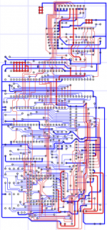
This is a progress image, NOT COMPLETE. I have removed a large number of items from my HD20's controller board in order to visually get the circuits copied. That's the only reliable way that I'm aware of, and I have absolutely found traces that split off into multiple traces beneath chips and connectors, things that I would not have found any other way. This data will be an invaluable tool to learn more about this drive, and I believe that it will lead to the emulation of this drive some day, even if it is beyond my abilities and/or patience. I am okay at de-soldering but not a pro, unfortunately... There are several lifted pads. xx(

This was a FUNCTIONAL HD 20. I think I'll get it to work again, but if not I still think that it's worth it. If anyone has a seized up HD 20, maybe we could work a deal. I don't really want to put this board back together because it's a great reference for us. Also, I will not touch my Rodime drive, I won't even risk removing the board from it. If I can get one that's seized up solid, I would be able to take the board off and chart it out like this controller board, and that could help us figure out some pins. I did some very limited continuity testing on my Rodime and found 2 pins that feed directly to schmitt trigger inverter inputs, so already we know that those 2 pins are input-only on the drive. Taking the board off of the drive and removing the chips could tell us a lot more. I have no idea where most of the pins connect on the Rodime.

Anyway, when I'm satisfied with this graphic, I will then begin to verify some things stated earlier in this thread and post my findings in a useful way, possibly on the wiki and/or my website.

Red = front

Blue = back

Seen from front.

Picture 1.png


Dennis Nedry

Well-known member
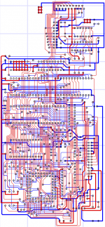
This image is complete but requires verification. I don't doubt that I missed a few lines. Some are very hard to see, for example, under a component I didn't remove or exactly under text/lines/etc. About half-way through, I discovered that if I put it up against my screen, the light shining through made the traces WAAAAY easier to see.

I am doing this in Osmond. It seems like an okay app for basically being free for this purpose. It's definitely not pro-quality, but it looks like it does okay. I'm open to suggestion if you know of some cooler PCB software on the freeware/shareware level. I've run into a few crashes and a few glitches after saving with this program, but nothing that I couldn't go back and touch up easily.

Picture 2.png


trag

Well-known member
Is that a two layer board? I ask because it looks like the Gnd and Pwr busses are made of traces, so I'm guessing there are no separate Pwr and Gnd layers.


Bunsen

Admin-Witchfinder-General
Dennis Nedry potentially sacrifices his HD20 controller board for the army...
I'm in awe.

I hereby nominate your HD20 for a citation for the MLA Purple Heart with full bars & clusters.


Dennis Nedry

Well-known member
Trag: Yes this is a 2-layer board. Holding the board up to a light source reveals no additional layers.

Bunsen: I totally agree, and that's the only reason that I could justify it. It also makes it more important to get something useful from this, so I'll be hard at work.


Dennis Nedry

Well-known member
Important discovery:

The Z8 processor is not on the main address bus, and consequently does not directly control the address of the RAM or ROM chips. And the large chip contains all of the possible address and data lines.

The Z8, IWM, and PAL share a common 7.5 MHz clock. This clock is not shared with the large chip.

7 of the Rodime pins are connected exclusively to the large chip, and 9 Rodime pins are connected to the Z8. Some of the Rodime/Z8 pins are also connected to the large chip. Many of these Rodime pins have pull-ups or series resistors.

The plot thickens...... How could the Z8 execute from ROM without direct access? If the Z8 does indeed execute from the ROM chip, there must be combinational logic contained in the large chip that allows the Z8 to look through it to the ROM. The alternative is that the Z8 isn't in fact ROM-less, and the ROM chip is used for some other purpose. It did disassemble into code that seems to make sense, so I still believe that it does execute from the ROM chip.


Gorgonops

Moderator
Staff member
Poor HD-20. I assume the ultimate goal is to lay this out into a 2D schematic? (With the IC's labelled and pin 1 marked?)

Completely off-topic, I happened to stumble upon a vintage computer mailing list post that mentioned in passing how the original Apple Profile drives worked: The short version is that conceptually the Profile drives were very similar to the Disk ][ drives, in that instead of buying "complete" drives from the manufacturer and using their specifications for the digital electronics Apple just bought bare mechanisms and "rolled their own" interface starting from analog up. (In the Profile's case said mechanisms were Seagate ST-506s and 412s.) Anyway, the post mentioned that there is a fair amount of documentation regarding the Profile drive on Bitsavers.org. Look here:

http://bitsavers.org/pdf/apple/disk/

The "Profile Level II Service Manual" goes into gruesome detail about how the Profile drive works, but... here are the bits that are interesting:

1: The Profile digital board used a Z8 CPU to implement the "high-level command set". That's an interesting coincidence, given the Z8 is also used in the HD-20 controller. And:

2: The names of the signals present on the connector between the Profile's digital and "Analog" boards almost exactly match the signals that are named on the patent document describing the Rodime 552 drive. Like... spookily the same. Reading the theory sections makes it sound as if the "division of labor" between the two boards is the essentially the same; In both systems there is a low-level MFM or RLL encoder on the "drive board" (MFM in the case of the Profile Analog board, RLL on the Rodime's board) that accepts serialized data from the "controller board" (via "READ DATA" and "WRITE DATA" lines for "/NRZ serial data"), both have "sys clock" lines (10Mhz for the Profile, 15Mhz for the Rodime, which makes sense for MFM vs. RLL")...

There are differences: In a spooky parallel to the difference between a Disk ][ floppy drive and a Macintosh floppy drive it *appears* to me that the Profile interface breaks out the raw stepper motor connections to the analog/digital interface, while the Rodime, with its own onboard Z8, accepts high-level commands for head positioning. (It says so much in the patent document.) But other than that I'd say with 90%+ confidence that the Rodime drive, for all its "specialness", is in fact just a slightly evolved version of the Profile (At least the mechanism+analog board portion of the Profile.).

As noted, there's substantial documentation for the Profile on Bitsavers; the parallel host protocol is well documented enough that More than one re-creation of it exists. The firmware files for the Profile's Z8 are on Bitsavers; it might be *very interesting* to dive into them and see if there are any matching blocks of code compared to the HD20's ROM dump. (Unfortunately there may *not* be that much similarity because of the differing head positioning protocols, but it still might be worth a look if you're really interested in the "Rodime" side of the code.) Complications with the IWM in place of the parallel interface aside I wonder if they might even use the same command set on the host side. (That's a Hail Mary, but you can always hope. The idea there would be is there's some jump table that vaguely matches between the two.) In any case, *somewhere* in the code is the command parser; if you can find it and can work backwards from that point to how it *receives* the command (IE, what torturous things happen between a byte erupting from the IWM's I/O port to that byte making sense to the command parser) you'll almost be at the goal posts.

Oh... Re: "Important discovery":

I would bet you a shiny new nickel that the biggest job that mystery chip does is serializing and deserializing data from/to a buffer in the RAM chip. (This job was mostly discrete hardware on the Profile, which means that chip is probably at least in part a single-chip condensation of the Profile's digital board.) Data will be spewing back and forth from the Rodime at 15Mhz and there's no way the Z8's going to handle that in software. The mystery chip undoubtedly has to put the Z8 on hold and use DMA to cram that data in and out of the RAM at warp speed. Meanwhile, the pins which are connected exclusively to the Z8 are almost certainly the control lines.

The patent doc has some signal names and partial schematics; it's *totally* unclear to me looking at any given partial schematic what the "P" numbers that show signals running off the page refer to. (It almost seems as if the schematics were intentionally partially obfuscated.) Does the (Rodime) board have any labels like "P1" next to its host connector? If it does, you could try matching those pins up to the the schematic fragments and see if, for instance, the serial read/write lines are indeed among those connected solely to Mr. Big Chip.

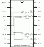
(EDIT: Profile Level II Service Manual, page 3.36. There's a block diagram. The top 1/3rd and right 1/2 of the diagram, including the shift registers, CRC generator, and Data MUXs... that's probably what's inside that big chip.)

 

Dennis Nedry

Well-known member
Here is the Osmond file (will open as text if you just click it normally, so save the link):

http://www.d.umn.edu/~bold0070/projects/hd20/HD20%20Schematic.osm

Thanks for the info Gorgonops.

I was honestly looking for a clearer distinction between Rodime-related parts and Floppy Bus-related parts, but it seems that everything critical has its fingers in that big mystery chip. I think that from this, we know how the daisy chain port works and how I/O is managed through the PAL. Beyond the IWM, a lot of assumptions have to be made, and I'm not sure if that's the easiest approach anymore.

I didn't label pin 1 or draw part outlines or any of that. Please use a photograph as a part reference at least for now. I'll probably put this board back together at some point. It might take an extra wire here or there but I'm pretty sure it'll be okay. I did not destroy the board by any means, and actually I have a couple sockets on order so that I can easily take the PAL and IWM chips back out as needed.

In one of the photos in the link you posted, Gorgonops, the controller board has a socket for the Z8 and PAL. This makes me wonder if the Z8 isn't ROMless - I can't imagine any reason to be pulling the Z8 out frequently. Also, underneath my Z8, it has "820-0157-A" printed on the board. None of the other chips have this.

Anyway, at this point with the mystery chip sitting squarely in the way, a Mac Plus HD 20 ROM hack might be a more appealing approach. We are basically dealing with serial data, an encoding scheme, and control lines. We have some idea of the function of the control lines from the HD 20 board. It seems reasonable that a great deal of information about the encoding can be learned from disassembling the Mac ROM.

 
Top