-
 Hello Guest! The forum software will be upgraded weekend of 06/26. See this announcement thread for more information.
You are using an out of date browser. It may not display this or other websites correctly.
You should upgrade or use an alternative browser.
You should upgrade or use an alternative browser.
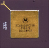
68040 mhz
- Thread starter konrad
- Start date
- Status
- Not open for further replies.


I would expect a late mask 040 to do 50mhz with ease but make sure you stick a good heatsink on it.
Newertech's Clockometer, part of the Gauge series.What tool or application is reliable for determining the actual MHz?
I've gotten E42K and 02E31F mask chips up to 57mhz on an accelerator. L88M/K63H around the same, 55mhz being the max I recalled. Earlier masks aren't reliable much past 33mhz under ideal conditions.
That said at these speeds the 040's bus drivers are well out of spec, there's no way you will attain anything close to these speeds on a complete system bus. If you have a normal fan and heatsink on the 040, that should be enough cooling for any speed it's able to do. Accelerators mostly have small buffered high speed busses so they can go a bit further without blowing timings. If you strapped the 040 into large buffer mode (greater drive strength) rather than the default small buffer mode you might get a hair more out of it, or removing extra RAM/ROM modules to reduce bus load.
Realistically, IMO, if you can manage a stable 45mhz on an 040 Mac I'd call it good.
For 030s, much past 60mhz gets wobbly on an unbuffered accelerator and 67mhz is the utter limit on a buffered accelerator. Same issues as the 040.
Has anyone ever achieved 50 MHz or more?I've gotten E42K and 02E31F mask chips up to 57mhz on an accelerator. L88M/K63H around the same, 55mhz being the max I recalled. Earlier masks aren't reliable much past 33mhz under ideal conditions.
That said at these speeds the 040's bus drivers are well out of spec, there's no way you will attain anything close to these speeds on a complete system bus. If you have a normal fan and heatsink on the 040, that should be enough cooling for any speed it's able to do. Accelerators mostly have small buffered high speed busses so they can go a bit further without blowing timings. If you strapped the 040 into large buffer mode (greater drive strength) rather than the default small buffer mode you might get a hair more out of it, or removing extra RAM/ROM modules to reduce bus load.
Realistically, IMO, if you can manage a stable 45mhz on an 040 Mac I'd call it good.
For 030s, much past 60mhz gets wobbly on an unbuffered accelerator and 67mhz is the utter limit on a buffered accelerator. Same issues as the 040.
@zigzagjoe just said that he’d successfully tested up to 55-57mhz.Has anyone ever achieved 50 MHz or more?
I was looking for information on the internet and I found this. http://centek.online.fr/atari/phenix/p_tech2.htm
According to this publication, the 040 cannot reach 50 MHz, is that true? RegardsI was looking for information on the internet and I found this. http://centek.online.fr/atari/phenix/p_tech2.htm
False? I can’t see where in the article it says that. The article just talks about Motorola’s marketing scam, advertising speeds with PCLK rather than BCLK. Many of us do run 040 chips up to and in excess of 50MHz - for example I am runnng my LC475 at 50MHz.According to this publication, the 040 cannot reach 50 MHz, is that true? Regards

Last edited:
Yup. And I overclocked my DayStar 68040 to 50 MHz.
Occasionally, DayStar 68K accelerators come up for auction on eBay. Sometimes the 50 MHz PowerCache 68030 card asking price will be higher than the sold price of some Turbo040 cards. Other times, you'll find both cards, but they'll be the slower versions. This post provides details on swapping out parts for a higher speed, and the overall performance of both cards at different frequencies.
I purchased a IIsi that included a DayStar P33 PowerCache 68030 card. The card was only at 40 MHz (rather than 50 MHz) and did not include the 68882 coprocessor.

There are three versions...
I purchased a IIsi that included a DayStar P33 PowerCache 68030 card. The card was only at 40 MHz (rather than 50 MHz) and did not include the 68882 coprocessor.
There are three versions...
- David Cook
- Replies: 3
- Forum: Mac II, Quadra & Centris
False? I can’t see where in the article it says that. The article just talks about Motorola’s marketing scam, advertising speeds with PCLK rather than BCLK. Many of us do run 040 chips up to and in excess of 50MHz - for example I am runnng my LC475 at 50MHz.
IMO it's a little more nuanced than "scam". My observations are that the 68040 behaves like a clock doubled 68030. Oversimplifying - but still -overall performance lines up disturbingly well with the 030 if you look at it that way, and it fits nicely with the common reasoning that an 040 is about twice as fast as an 030 clock-for-clock.
The caveat with that argument is to run an 030 at peak performance demands too much of the rest of the system with the technology of the time. A segmented (buffered) bus with L2 cache is mandatory, and you *still* get hosed on writes unless you do something exotic with your DRAM. Aka, take a look at the IIfx and the resulting mess. The massively improved write back cache of the 040 allowed keeping the CPU appropriately fed with a more sedate (economical) system design. Of course, there were other improvements - namely the bus interface and FPU - but the CPU core itself I don't think was much improved beyond that.
My guess is it was more of a political discussion. At the time (1990), bus clock was synonymous with CPU clock speed.... while using the PCLK for advertising gives a nice "big number = better" it also means the IPC isn't much improved over the 030. If your "50mhz" 68040 is going head to head with a 25mhz 486 ... that's really not a good look. Think of Pentium 4's ridiculous clock frequencies but relatively poor real-world performance. Using the lower number implies that the IPC (and design) is much improved and perhaps also suggests that the chip might scale frequency further over the lifetime of the design than it otherwise might due to limitations. Just splitballing, though.
That article seems to be dissecting motorola's advertised instruction timings and I do think something weird was done with those, both with 040 and 060. In the 68060 thread I've a post disussing that. I'm still not entirely sure I didn't make a mistake somewhere, as these are complex chips with complex timings, but I'm pretty sure motorola was playing games with that data. Weither it was intentional or "simply" obfuscated by complexity is perhaps the question.
What I don't understand is that Motorola was manipulating data against the competition. I saw the image; it says approximately 50 MHz. Is that tool reliable? Thanks for listening.False? I can’t see where in the article it says that. The article just talks about Motorola’s marketing scam, advertising speeds with PCLK rather than BCLK. Many of us do run 040 chips up to and in excess of 50MHz - for example I am runnng my LC475 at 50MHz.
View attachment 94830
YesWhat I don't understand is that Motorola was manipulating data against the competition. I saw the image; it says approximately 50 MHz. Is that tool reliable? Thanks for listening.
Not really a scam. Marketing needs and all-around misunderstanding of how CPU works I'd say.IMO it's a little more nuanced than "scam"
WayWayTL;DR: That, and see the last few paragraphs, after all the long historical and near-technical ramblings.My guess is it was more of a political discussion. At the time (1990), bus clock was synonymous with CPU clock speed
It's the same issue as the whole "that's an 8-bits computer and that's a 16-bits computer and ...". CPU are complicated beasts, but people like simple measurement that can be fully ordered... I don't think anyone think the original Core i7 where 192-bits computers just because their external bus had 3 64-bits channels. Let alone than 5th gen AMD Epyc as 768-bits. "CPU frequency" is nearly as much an oversimplification and means not much (spoiler alert!).
Originally for personal computers, clocks were fairly low and no-one that wasn't ITB or a motivated hobbyist knew what a clock was - frequency what the thing you tuned to on the dial of the radio. And the width of the bus was a critical aspect for performance as everything went through that interface (no caches!) and doubling the width pretty much doubled the performance. Early home computers had a 8-bits bus because that was cheap. The other important thing was memory size; memory was expensive (the more things change...), so that was a critical aspect. If you look at early Apple II ads, they don't mention frequency (just "6502 processor"), they do mention the size of the RAM chips - both in KiB and physical: what package they use!. Frequency was in the datasheet and user manual so companies could build a system with those CPUs.
Originally it was a bus width war with the so-called "16-bits" (mostly the MC68000, though it now [w|sh]ould be considered a 32-bits CPU given the width of registers and pointers, plus some outliers like the TMS9900) system trying to push aside the 8-bits systems. But still, the thing that mattered was bus width and memory - even though the mention of clocks (after all the 8 MHz of the '000 could be mentioned against the common 2 to 4 MHz of the Z80, even if it didn't mean anything to anyone) was there now.
The frequency was didn't really pick up before the i80386, though the i80286 had started the discussion. There were machine with the smae CPU but two (or more) different levels of performance based on that new-fangled marketing buzzword, "CPU frequency"! That was marketed heavily, and that wouldn't stop for a couple of decades. But at that point, as @zigzagjoe said, the one advertized frequency was the one that mattered to system builders - the bus frequency. Whatever happened inside the CPU, stayed inside the CPU, same for the MC68040 as for its predecessors (spolier alert!).
Of course comparing clocks between microarchitectures is absurd, but that never stopped anyone doing it. There's plenty of benchmarks of the era where the ranking between microarchitectures is mostly independent of clock speed, even if clock speed allows for perfect ordering of a single micro-architecture (read: faster is better... for the same silicon).
Now back to the MC68040; it was originally sold with the bus frequency as its "CPU frequency". That's the frequency ssystem builders needed to target to build a system (timings of memory and other devices on the system bus), so it made sense. They just had to remember to add that pesky MC88916 for the PCLK... and at the time, nobody thought anything of it. The MC68040 was faster than the i80486, wasn't it? What else mattered? And what is that "clock for clock" mention there?!?
Well the marketing clock mattered, in particular after the introduction of the DX2 variant of the 486. So at some point people at Apple and/or Motorola (or somewhere) looked at the MC68040 user manual and saw this gem in it (section 7.1):
Meaning, at least some of the logic is running out of the phase-locked variant of PCLK (to the BCLK). Incidentally, the MC68040V and several other variants don't have a PCLK fed to them; some interpret this as meaning it's not used. Except the '040V still has all the PLL power pins, and odds are, the PLL is also acting as a built-in frequency multiplier in addition to the phase-locking in the '040V. That's just a small part of what the MC88916 could do that needed to be integrated, and the PLL was already there anyway.The use of dual clock inputs allows the bus interface to operate at half the speed of the internal logic of the processor
So we ended up with the "33/66 MHz" "CPU frequency" advertising for the MC68040... and closing on four decades of discussion of whether that's legit or not. Which, to me, is discussing how many angels can dance on the head of a pin.
(a) some of the logic is clocked at PCLK (otherwise they wouldn't say so let alone have bothered with adding the pind and the PLL, that's some complicated analog stuff to add for no reason to a digital design), so it is correct
(b) some of the logic (e.g. at least the bus interface) is clocked at BCLK, so it is incorrect
(c) the exact same two arguments can be used for/against the i80486DX2 and DX4
The problem is that for the 486, it was probably fully synchronous to the bus clock originally (similar to what would later be called a "Brainiac" - do more each cycle, lower frequency) while the MC68040 had some parts running faster than the bus (similar to what would later be called a "Speed Demon", just push the clock by simplifying each stage of the pipeline). So when Intel added the ability to run at twice (later 2x and 4x) the bus speed, it was natural to keep the internal clock as the "CPU frequency" even if the bus clock was only half as much. But for Motorola, they had started advertising the bus clock as the "CPU frequency" with the internal clock being purely technical, and it felt like a cheat when it was added to the marketing material - this new number was double the old one, but that didn't change anything to performance because it had always been there...
As for measurremnt to figure out the "truth" (as if there was truth in marketing!), the only observable thing from the outside is the bus clock, so any measurement is going to return whole bus clock cycle values. Whether an instruction takes 5 BCLK cycles or 9 or 10 PCLK cycles, externally it will be observed identically. And it's likely Motorola did the pipelining with even number of stages for everything, as it makes things a lot easier if you always change clock domains between phase-locked clocks on the destination clock edges - no need for delays, resynchronization or CDC, just move from one to the other seemlessly (the curve25519 crypto engine does that with 3 clocks at nominal, nominal/2 and nominal*2).
Again, @zigzagjoe mentioned the MC68040 looks a lot like a clock-doubled MC68030 (with extra caches). One could esaily speculate it's because it's essentially what it is. Most of the instructions takes about half the number of cycles at BCLK on the '040 as they do on the '030... or maybe they didn't massively improve every aspect of the micro-architecture between generations, they just clocked most of the existing one with PCLK, and added a BCLK-clocked interface to the bus and maybe some internal part of the CPU that were too cumbersome to run at PCLK (maybe the caches, etc.). But thas is all speculation. If only Motorola had told us...
[actual answer starts here
") ]
]... which of course, they totally did. The explanation was published in 1990 in a IEEE conference.
- Is she '040 ALU is effectively clock-doubled vs it's predecessors? Yes.
- So it is running at double the bus clock? No! It's just ... no longer running at half speed

[the '030 is essentially the same as the '020 for this]
The "fast" clock (CLK for the '020/'030, PCLK on the '040) is used for various timings between the internal ALU which is running at the slow clock (CLK/2 for the '020/'030, BCLK on the '040) and the bus which is running at the external clock (CLK for the '020/'030, BCLK for the '040).
So if the MC68030 @ 25 MHz is a 25 MHz processor, then is a MC68040 @ 25 Mhz a 50 MHz processor by virtue of running its ALU at double the frequency of the MC68030? Or is the lie that the MC68030 @ 25 MHz should have been called a 12.5 MHz all along?
How many angels can dance on the head of a pin? None, as there's no such things as angels.
What it the "CPU frequency" of a MC68040 ? None, as there's no such thing as a "CPU frequency".
- Status
- Not open for further replies.
Similar threads
- Replies
- 14
- Views
- 917