• Hello MLAers! We've re-enabled auto-approval for accounts. If you are still waiting on account approval, please check this thread for more information.

The most horrible USB card layout I’ve ever seen

Knowing a bit about USB 1.1 interfaces now, I thought I’d share images of this card I got off eBay sold as working. It has no inline ferrite beads on the data lines or fuses on Vbus, basically no form of hot plug/overcurrent protection at all. Two of the traces on the back have burned through!

Also, most cards like this have lots of 100nF filter caps connected to the USB chip, whereas this card has none.

The designers can’t have just overlooked the datasheets, they must have known what they were doing.
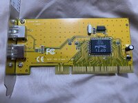
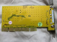
IMG_9555.jpeg
IMG_9556.jpeg
 
True Story: A bunch of big name motherboard makers decided to skimp on ESD protection on their USB ports when building Intel i865 based boards. Enough of them blew up that a recall had to be issued.
 
I like the surface-mounted through-hole capacitor.
Oops, it actually is through-hole mounted, my bad!
 
That is what "built to a price" looks like. Also, if that's really version 7.0 I'd hate to see the first 6.
 
i'm just sleepingly joking (yeah i need to go to bed very soon so..) but I wonder if the very first version maybe had absolutely nothing but just the one lone opti ic chip alone on it? talk about trying to figure how little to get away with in a somewhat weird way to do it?
 
I was looking again at this board and was wondering: Got ground plane? That's a bigger ground plane than a small Serbian village. Maybe we should route the +5V and GND over those.
icon_mrgreen.gif
Shirley it won't burn up the host motherboard trying to draw 20 Amps through it?
 
I was looking again at this board and was wondering: Got ground plane? That's a bigger ground plane than a small Serbian village.

Any cuts to the PCB that aren't to meet the PCI spec add cost and manufacturing complexity, so it's a big empty rectangle. Same idea with not etching most of the copper layer, probably.
 
Knowing a bit about USB 1.1 interfaces now, I thought I’d share images of this card I got off eBay sold as working. It has no inline ferrite beads on the data lines or fuses on Vbus, basically no form of hot plug/overcurrent protection at all. Two of the traces on the back have burned through!
Plot twist: the traces ARE the overcurrent protection :LOL:
 
Oh I'm aware that the more traces you plot into your board the more expensive it is. I was just being sarcastic.
 
I was a Manufacturing Engineer in the PCB business for many years. My opinion is someone has intentionally applied WAY more current to that board than was required. 500 mA at 5V (USB maximum) will not blow those large traces off the board. You need about 100V at 15 Amps to do that kind of damage.
 
Back
Top