I know -- hardest to repair, however this board was actually in pretty good nick ,as this is my first logic board repair ever I'm being overly pedantic so could rely appreciate a bit of wisdom from all the re-cappers here who have done hundreds of them
The board originally had visible electrolyte leakage around the SMD electrolytics. I removed the PRAM battery, removed the logic board, cleaned it with IPA, and removed all wet electrolytic caps. The board is now much cleaner, but I ran into a few pad issues during cap removal.
Confirmed logic-board cap list:
- C1, C2, C4, C5, C6, C8, C9: 47uF 16V
- C3: 1uF 50V
- C7 and C10 appear to be tantalum chip caps, so I am leaving them alone
Replacement parts I have ready:
- Panasonic aluminium polymer SMD caps for the 47uF positions
- KEMET C1206C105K5RACTU 1uF 50V X7R MLCC for C3
Known damage / questions:
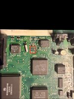
C2
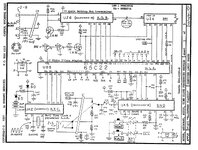
I lifted/lost the negative pad on C2 during my first cap removal attempt. Looking at the BOMARC schematic, C2 appears to be in the UA5/SND area and the negative side goes to ground. My plan is to install the new C2 with the positive side on the remaining positive pad and run a short 30AWG jumper from the new capacitor negative terminal to a verified ground point.
Does that sound like the correct repair for C2 on this board?
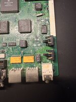
C3
C3 is the 1uF 50V cap near UA5/SND. I removed it after the others and both pads are mechanically suspect. They still appear to exist, and at least the ground-side pad tested electrically connected at one point, but I do not fully trust them as mechanical anchors.
Since I am replacing C3 with a small non-polar MLCC, my current thinking is:
- if the pads are still electrically valid, solder the MLCC very gently
- if the ground-side pad is unreliable, jumper that side to verified ground
- if the SND-side pad is unreliable, jumper that side back to the proper UA5/SND node, not ground
- add mechanical strain relief only after electrical repair/testing, not as the primary repair
Is that the right way to think about C3?
C4
This is the confusing one. C4 looks visually fine to me, but the negative pad does not test like ground.
Meter readings after cleaning, board unpowered:
Other known ground/negative pads -> known ground: about 0.1 ohm
C4 positive pad -> known ground: about 35.7 ohms, steady
C4 negative pad -> known ground: about 2 Mohms and climbing quickly
Nearby via on the C4-positive side -> known ground: about 0.1 ohm
C4 positive pad -> that nearby via: about 36.6 kohms
C4 negative pad -> that nearby via: about 2 Mohms
So my interpretation is:
- the nearby via is a valid ground point
- that via is not directly connected to C4+
- C4- has lost its ground connection, even though the pad looks physically intact
My planned repair is:
new C4 negative terminal -> short 30AWG jumper -> nearby verified ground via
Then verify:
C4 negative -> ground: near 0 ohms
C4 positive -> C4 negative: not a short
Does this diagnosis make sense? Is there a known hidden/via/trace failure around C4 on Macintosh Classic 820-0390-B boards, or am I missing something about how this cap is connected?
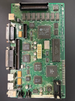
Photos attached:
- full board photo
- C2 damaged pad photo
- C3/C4 area photo
- relevant schematic page/crop
Any advice before I install the replacement caps and jumper repairs would be appreciated. I am trying to do this slowly and not make the board worse.
The board originally had visible electrolyte leakage around the SMD electrolytics. I removed the PRAM battery, removed the logic board, cleaned it with IPA, and removed all wet electrolytic caps. The board is now much cleaner, but I ran into a few pad issues during cap removal.
Confirmed logic-board cap list:
- C1, C2, C4, C5, C6, C8, C9: 47uF 16V
- C3: 1uF 50V
- C7 and C10 appear to be tantalum chip caps, so I am leaving them alone
Replacement parts I have ready:
- Panasonic aluminium polymer SMD caps for the 47uF positions
- KEMET C1206C105K5RACTU 1uF 50V X7R MLCC for C3
Known damage / questions:
C2
I lifted/lost the negative pad on C2 during my first cap removal attempt. Looking at the BOMARC schematic, C2 appears to be in the UA5/SND area and the negative side goes to ground. My plan is to install the new C2 with the positive side on the remaining positive pad and run a short 30AWG jumper from the new capacitor negative terminal to a verified ground point.
Does that sound like the correct repair for C2 on this board?
C3
C3 is the 1uF 50V cap near UA5/SND. I removed it after the others and both pads are mechanically suspect. They still appear to exist, and at least the ground-side pad tested electrically connected at one point, but I do not fully trust them as mechanical anchors.
Since I am replacing C3 with a small non-polar MLCC, my current thinking is:
- if the pads are still electrically valid, solder the MLCC very gently
- if the ground-side pad is unreliable, jumper that side to verified ground
- if the SND-side pad is unreliable, jumper that side back to the proper UA5/SND node, not ground
- add mechanical strain relief only after electrical repair/testing, not as the primary repair
Is that the right way to think about C3?
C4
This is the confusing one. C4 looks visually fine to me, but the negative pad does not test like ground.
Meter readings after cleaning, board unpowered:
Other known ground/negative pads -> known ground: about 0.1 ohm
C4 positive pad -> known ground: about 35.7 ohms, steady
C4 negative pad -> known ground: about 2 Mohms and climbing quickly
Nearby via on the C4-positive side -> known ground: about 0.1 ohm
C4 positive pad -> that nearby via: about 36.6 kohms
C4 negative pad -> that nearby via: about 2 Mohms
So my interpretation is:
- the nearby via is a valid ground point
- that via is not directly connected to C4+
- C4- has lost its ground connection, even though the pad looks physically intact
My planned repair is:
new C4 negative terminal -> short 30AWG jumper -> nearby verified ground via
Then verify:
C4 negative -> ground: near 0 ohms
C4 positive -> C4 negative: not a short
Does this diagnosis make sense? Is there a known hidden/via/trace failure around C4 on Macintosh Classic 820-0390-B boards, or am I missing something about how this cap is connected?
Photos attached:
- full board photo
- C2 damaged pad photo
- C3/C4 area photo
- relevant schematic page/crop
Any advice before I install the replacement caps and jumper repairs would be appreciated. I am trying to do this slowly and not make the board worse.