• Hello MLAers! We've re-enabled auto-approval for accounts. If you are still waiting on account approval, please check this thread for more information.

Socketed SE/30 PowerCache HiRes pics needed. HELP!!!!! ;-)

Trash80toHP_Mini

NIGHT STALKER
68040
Thanks to BadGoldEagle's quick response, I have a nice photo of the socketed version of the PowerCache SE/30. Now it's time to ask for more help!

1) HiRes photo of just this section - please, please, please!

2) Same for the solder side - wishful thinking, not expecting removal/re-installation of such a valuable board.

3) Buzzed connections - pipe dream there - might be some risk involved?
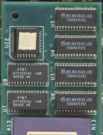
Socketed_PowerCache.00.jpg

It looks for all the world to me that the PAL(? Component U22) is re-mapping the address location of the Cache so as to relieve conflict with the SE/30's Video Subsystem located @ PseudoSlot $E.

9107747564_4591a19e6e_b.jpg.bbf08e12c62ca4a5283b105c7d1b0a64.jpg


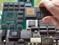
Found a curious difference between my socketed and non-socketed versions of the SE/30 board.

SE30-socketed-ICs.JPG

The five ICs directly under James Wages' thumb are socketed on his board and on my socketed CPU board as well. On my stock logic board, those five ICs are soldered directly to the board along with the CPU.

I've also got a patch wire on my socketed board running from a blind via between the right side pair of socketed ICs and soldered to the third leg of the Socketed IC (U16) on the left in group of five in the pic above. That chip is definitely staying in place! 8-o

Are those five ICs commonly implemented in sockets on socketed CPU SE/30 boards?

Are they normally soldered to the mobo of stock SE/30s?

Did some SE/30s come with socketed CPUs from the factory?

DayStar did a lot of Socket conversions to stock boards IIRC.

Has anyone noticed these or any other differences between board types?

Looks like credit for the top pic goes to JW's beautiful documentation as well.

 
The GAL next to the cache is part of the cache comparator.

The cache just hangs on the address and data bus and is not directly addressed as cache. Stuff is just written to cache on RAM write operations. The TAG RAM next to the SRAM stores the main memory addresses of whatever is put into the cache.

If a read operation is taking place the 030 puts the address on the bus that it wants to read from and if things the CPU wants to load are also in cache the TAG RAM will have the corresponding main memory address stored and signal the GAL that the data the CPU wants to read is also in cache.

The GAL will then enable the SRAM outputs and terminate the read cycle as soon as possible. The read cycle termination would normally be done by the GLU once data is ready to be read from RAM.

 
Last edited by a moderator:
OOPSie!  [:O] My bad!

I meant the five socketed ICs down on the SE/30's logic board positioned below the thumb in the pic, not the ICs directly under his thumb on the PowerCache.

 
I was referring to that:

It looks for all the world to me that the PAL(? Component U22) is re-mapping the address location of the Cache so as to relieve conflict with the SE/30's Video Subsystem located @ PseudoSlot $E.
explaining that it is not remapping any addresses ;)

I have a few different SE/30 logicboards. There are ones with socketed video subsystem ICs from the factory.

All my boards have soldered CPUs. Also there are boards that have a socketed CPU from the factory but then again not all of those have socketed video chips.

 
Aaaah! Didn't really read the my IP, just appended the new info request. Thanks for correcting my misconception.

It's amazing how far and fast you and joe have run with PowerCache adapter development. It's less than a year since I requested pics! Thanks for explaining the function of the ICs on PowerCache and SE/30 board, I was curious about that. So the GALs on the adapters prevent conflict at the control line level overall and not about memory conflicts with Slot $E video after all?

I discovered the socketed ICs on my socketed mobo while checking clearances for using the CPU socket interface for a 10cm x 10cm prototyping card:

Socketed SEEED Board SE30.JPG

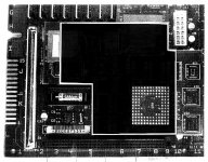
Had some downtime at work and knocked together a quick pasteup using the first pic in this post. I was idly thinking in terms of your accelerator development research when I ran across a pic of the PowerBook 100 processor daughtercard I'd snagged somewhere. That led back to ancient notions for the Portable Performer PDS transplant and PowerBook 100 spinoff. In that new project thread you mentioned the Amiga crowd's TerribleFire accelerator. Looked at that last night and suddenly I'm back to the socketed protoboard notion again. The noggin's running around in circles. :blink:

I'll bet a pretty penny you've been thinking along these lines already, B!  [;)]

 
Last edited by a moderator:
Back
Top