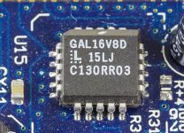
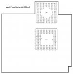
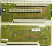
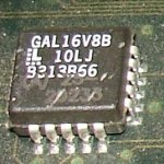
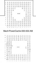
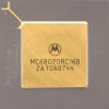
A long time ago in a lifetime far removed, mcd and I were talking about the PowerCache Adapter Cloning project. On a hunch, I figured that teasing apart the signals on his Macintosh II adapter between discrete 68020 and MMU components and the IIci cache slot might be very useful in gaining an understanding of the much "simpler" 68030 PDS adapters. So he sent it along to me and I dug it out from under the heap yesterday:
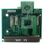
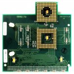
*Solder side mirrored to match topside.*
Plan of attack is to de-solder all components and re-create all traces leading to the three ICs and then those heading out to the IIci Cache Slot Adaptation in Illustrator as usual. I'm going to add a new twist to the process this time around though. I'm planning to spread the ICs out a bit so I can label them like in a "real life" schematic diagram for those of you who are good at deciphering such things. That way someone might be able to help me without needing to decipher my visually oriented artwork schematics.
So, whatcha think,? Am I possibly right in guessing that this will turn out to be illuminating as to the processes of the PowerCache adaptations?

