So, a few months back I read this post: link by the great Trag, and started researching how to upgrade the stock ATi Rage II based video on my PowerMac 6500 board.
I PM'd Trag and we discussed a bit on the possibility to double the VRAM of the PM 6500, a possibility that would open interesting scenarios.
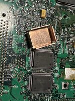
This can be accomplished by replacing the 1mb SGRAM chips on the logic board with 2mb parts - - for a total of 4MB.
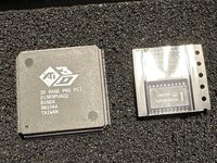
So, Jeff graciously sent me a few KM4132G512Q-10 chips, they're 256 X 32 X 2 (2MB) each, while the chips already soldered on the 6500 are MT41LC256K32D4, 128 X 32 X 2 (1MB). I am adding both Data Sheets below.
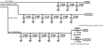
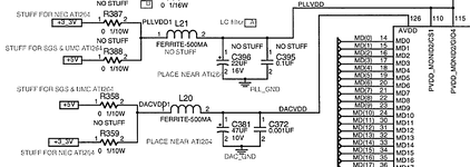
While the pin for BA, according to the 6500 schematic, is connected (they are both dual bank chips) the caveat here is that address lines A8 and A9 are, for some unfathomable reason, mapped on different pins on the MT and KM memory chips footprint which are otherwise essentially the same.
I will undoubtedly have to bodge some wires to solve this.
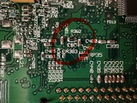
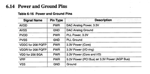
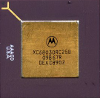
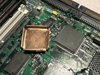
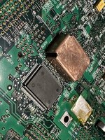
But, studying the data sheets of both memory chips, I realized I needed to know about the Rage II video chip to know where to place those bodges. Yes, the ATi Rage II in the 6500 schematic features pin labels, but I needed to know how the chip worked.
It turns out no data sheet is available anywhere online for the Rage II... but there's a technical reference manual for the Rage Pro! And I found out that, in the PCI compatible, PQFP 208 package implementation, it is a direct, pin to pin compatible part, meant to simplify upgrading existing designs of integrated M/B graphics built around the Rage II.
So, it is possible that it is a drop in upgrade for the 6500 board, adding substantial performance (at least double the acceleration, plus much better 3D games compatibility and much more). Well, let's say that at least, it should equal the video performance of the beige G3, that incidentally uses the Rage pro...
This more or less sums up the research I did, however impossible to do otherwise without Trag's input and help.
I PM'd Trag and we discussed a bit on the possibility to double the VRAM of the PM 6500, a possibility that would open interesting scenarios.
This can be accomplished by replacing the 1mb SGRAM chips on the logic board with 2mb parts - - for a total of 4MB.
So, Jeff graciously sent me a few KM4132G512Q-10 chips, they're 256 X 32 X 2 (2MB) each, while the chips already soldered on the 6500 are MT41LC256K32D4, 128 X 32 X 2 (1MB). I am adding both Data Sheets below.
While the pin for BA, according to the 6500 schematic, is connected (they are both dual bank chips) the caveat here is that address lines A8 and A9 are, for some unfathomable reason, mapped on different pins on the MT and KM memory chips footprint which are otherwise essentially the same.
I will undoubtedly have to bodge some wires to solve this.
But, studying the data sheets of both memory chips, I realized I needed to know about the Rage II video chip to know where to place those bodges. Yes, the ATi Rage II in the 6500 schematic features pin labels, but I needed to know how the chip worked.
It turns out no data sheet is available anywhere online for the Rage II... but there's a technical reference manual for the Rage Pro! And I found out that, in the PCI compatible, PQFP 208 package implementation, it is a direct, pin to pin compatible part, meant to simplify upgrading existing designs of integrated M/B graphics built around the Rage II.
So, it is possible that it is a drop in upgrade for the 6500 board, adding substantial performance (at least double the acceleration, plus much better 3D games compatibility and much more). Well, let's say that at least, it should equal the video performance of the beige G3, that incidentally uses the Rage pro...
This more or less sums up the research I did, however impossible to do otherwise without Trag's input and help.
Attachments
Last edited:
")