Trash80toHP_Mini
NIGHT STALKER
. . . has become my current obsession.
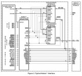
Since my project to hack the IIsi NuBus Adapter onto the PDS appears to require bus mastering expertise I'm not likely to acquire, removing the NuBus MUX and to dumb a card back down to I/O bus spec seems the best way to approach this.
Target is the SE/30's 68030 socket and I've got both ThinNet and 10bT daughtercards for my pair of Futura's, so that's an added bonus if I can grab the brass ring.

Looks like the wedge would be the pads for the output side of theoe two SMT MUX ICs.
I've got a 10" color CRT headed into the extra SE/30 case sometime soon. The monitor supports the two resolutions in bold. Removing the A/B and possibly the Original equipment PSU sheet metal surround for the ATX PSU conversion makes for area/cubic requirements for the monitor's guts.
Barring complications elsewhere, pulling the Video ROM may free up onboard video's PseudoSlot $E interrupt for the card. It definitely makes the Video Subsystem on that interrupt disappear from Slot Manager's watchful eye.
Yeah, I know about the CRT neck length thing, but I cheat really neat. [} ] ]'>
] ]'>
Since my project to hack the IIsi NuBus Adapter onto the PDS appears to require bus mastering expertise I'm not likely to acquire, removing the NuBus MUX and to dumb a card back down to I/O bus spec seems the best way to approach this.
Target is the SE/30's 68030 socket and I've got both ThinNet and 10bT daughtercards for my pair of Futura's, so that's an added bonus if I can grab the brass ring.

Looks like the wedge would be the pads for the output side of theoe two SMT MUX ICs.
lowencmac:
The card provides standard QuickDraw acceleration and supports the following resolution/color combinations:
E-Machines Futura cards have a rotary switch for setting the resolution. The following is a list of switch settings. This setting is overridden when using a supported monitor with Apple's sense coding.
- 640 x 480 up to 24-bit
- 832 x 624 up to 24-bit
- 1024 x 768 (at 75 Hz) up to 8-bit
resolution refresh monitors
1 832 x 624 67 Hz T16
2 1024 x 808 71 Hz T19/TX
3 640 x 480 60 Hz any VGA
4 1024 x 768 60 Hz any XVGA
5 832 x 624 75 Hz T16a-E16
6 1024 x 768 75 Hz E16, SuperMac 19", others
7 640 x 480 67 Hz E16, others
8 1024 x 768 75 Hz RasterOps 19", others
C 13"/16" Dual Resolution E16
D 16"/19" Dual Resolution T16II/E16
E 19"/21" Dual Resolution T19II
F 16"/21" Dual Resolution T16II
I've got a 10" color CRT headed into the extra SE/30 case sometime soon. The monitor supports the two resolutions in bold. Removing the A/B and possibly the Original equipment PSU sheet metal surround for the ATX PSU conversion makes for area/cubic requirements for the monitor's guts.
Barring complications elsewhere, pulling the Video ROM may free up onboard video's PseudoSlot $E interrupt for the card. It definitely makes the Video Subsystem on that interrupt disappear from Slot Manager's watchful eye.
Yeah, I know about the CRT neck length thing, but I cheat really neat. [}
Last edited by a moderator:


