• Updated 2023-07-12: Hello, Guest! Welcome back, and be sure to check out this follow-up post about our outage a week or so ago.

Apple Techstep I have almost all of the ROMs here and some info!

elemenoh

Well-known member
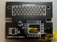
I was able to mod the board as @SuperSVGA instructed and it did indeed work!

Here's how I went about it.

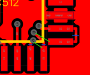
1. Cut the traces as advised above and tested for continuity
2. Scraped the mask off of the affected vias
3. Placed 40AWG enameled wire into place and secured it with kapton tape
4. Soldered the socket, starting with the bodges
5. Trimmed off the excess with a hobby knife

Note I did the above under a microscope. This would be a lot harder without one.

It was a little fussy to do, but came out fine. Reworking the already built boards will be a bit more of a challenge because the sockets need to be removed first.

IMG_1542.jpeg
IMG_1548.jpeg
 
Last edited:

elemenoh

Well-known member
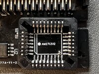
Here's a reworked cartridge. The PLCC socket was a PITA to remove but did eventually let go. The main fallout was that a couple areas lost a bit of solder mask.

This is what I did to get the socket off:
1) Sopped up as much solder with wick as possible.
2) Placed a hobby knife on the side with U2, using that as a fulcrum.
3) Heated the pins on that side until there was enough space to fit a small flathead screwdriver where the knife was.
4) Worked from left to right heating up pins to create a larger and larger wedge and eventually removed the connector.

Rework of the board itself was identical to the previous post. This one tested fine after rework too.

IMG_1555.jpeg
 

jajan547

Well-known member
Here's a reworked cartridge. The PLCC socket was a PITA to remove but did eventually let go. The main fallout was that a couple areas lost a bit of solder mask.

This is what I did to get the socket off:
1) Sopped up as much solder with wick as possible.
2) Placed a hobby knife on the side with U2, using that as a fulcrum.
3) Heated the pins on that side until there was enough space to fit a small flathead screwdriver where the knife was.
4) Worked from left to right heating up pins to create a larger and larger wedge and eventually removed the connector.

Rework of the board itself was identical to the previous post. This one tested fine after rework too.

View attachment 39785
Actually turned out quite nice, looks great @elemenoh.
 

SuperSVGA

Well-known member
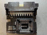
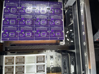
Here's the fixed 512Kbit boards attached.


My 1Mbit panels finally arrived. Next time I'm making smaller panels...
IMG_3229.jpg
 

Attachments

  • Gerber_PCB_TechStepCart1 M95020_2022-03-23.zip
    37.9 KB · Views: 6
  • Gerber_PCB_TechStepCart1_2022-03-23.zip
    38.6 KB · Views: 8

jajan547

Well-known member
Please use this newest folder it's much easier and simpler to follow.
 

Attachments

  • Everything Apple TechStep.zip
    11.2 MB · Views: 4

jajan547

Well-known member
Forgot to add the updated Gerber fix for the 512k board both through hole and SMD have been fixed and are in this 2.1 Folder.

Thank You To @pocketscience for the catch.
 

Attachments

  • Everything Apple TechStep 2.1.zip
    11.2 MB · Views: 10

sarnau

Member
FYI: I am currently looking into the firmware for the TechStep and based on that I add a few potentially interesting things:
  1. You can use the 128k ROMs (maybe even 256kb ones, TechStep supports up to 8 banks) for any TechStep ROM Pack. They are bank-switched into the address space, additional unused memory is simply ignored by the code. There is no need for custom 64kb ROM Packs, they are simply the older ones.
  2. The 2kb I2C EPROM is not necessary to use the ROM Pack. The _only_ time it is accessed, is when you want to save/show a Log into/from the ROM Pack instead of leaving it in memory. If you never do that, you can ignore that chip. On the other hand: it costs almost nothing to add it.
  3. The content of the I2C EPROM is writing during save. By default there is no data in the I2C EPROM.
 
Top