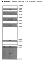
Now comes the part of choosing the new address ranges to relocate them!
Any suggestion?
To differentiate RAM access from ROM/SCSI accesses in those ranges seems easy to solve (using FC2, FC1, FC0, perhaps?).
Also, I guess something has to be done differently when OVERLAY is asserted.
Also, the changes to the RAM expansion board to have 8MB are minimal. The whole thing feels feasible, once you have the CPU on a daughterboard!
Depends on how much RAM you want to add. What you would want to do is change where the CPU thinks the memory locations are (i.e. edit the ROM to change their locations) but the logic board would need them accessed from the same location.
For example how I would do it:
- RAM, ROM, a 68000, and the logic on the expansion card.
- Bus transceivers for the address lines, with the /OE controlled by NAND logic from A20, A21, A22, and A23. That way all accesses from
0x000000through0xEFFFFFdo not reach the logic board. - Address lines A19, A20, A21, A22, and A23 to the logic board generated by the expansion card's logic to recreate accesses to the logic board's memory map at the right locations.
- Put all the peripherals on the bus between
0xF00000through0xFEFFFFfrom the CPU expansion card's side, which will be converted to the correct addresses on the logic board.


