• Hello MLAers! We've re-enabled auto-approval for accounts. If you are still waiting on account approval, please check this thread for more information.

Mac Plus 68020 Accelerator

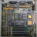
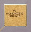
I'm adding a full view picture of the logic board. Ignore the ROMs, they are from a Plus. I also added a 68000 CPU following @Bolle suggestion, though no further progress with it.

Is it normal that the LBs of the Plus have a diode factory installed at CR1? I thought not (as it would provide termination power to SCSI, if I'm not mistaken, a mod I noticed a few months ago being discussed).

Is there anything else the community sees here of unusual nature?
IMG_2893.jpg
View attachment IMG_2894.jpg
 
I'm adding a full view picture of the logic board. Ignore the ROMs, they are from a Plus. I also added a 68000 CPU following @Bolle suggestion, though no further progress with it.

Is it normal that the LBs of the Plus have a diode factory installed at CR1? I thought not (as it would provide termination power to SCSI, if I'm not mistaken, a mod I noticed a few months ago being discussed).

Is there anything else the community sees here of unusual nature?
View attachment 81535
View attachment 81536
That’s not a Motorola 68000 - it’s second-sourced, right?
 
Were there any new developments regarding this mystery accelerator? If the function of those other ICs could be determined, this seems like it would be relatively easy to reverse engineer and manufacture!
 
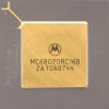
If CPU and FPU (marked 12MHz?) are really only running at 12MHz it's no wonder nobody has seen this thing. It would then only be half the performance kick of the 16MHz Performer that we've already cloned. When was the 16MHz 68020 released? Radius16 was one of the first Accelerators for the Mac.

Flash in the pan, if that at 12MHz? 😒
 
Last edited:
If CPU and FPU (marked 12MHz?) are really only running at 12MHz it's no wonder nobody has seen this thing. It would then only be half the performance kick of the 16MHz Performer that we've already cloned. When was the 16MHz 68020 released? Radius16 was one of the first Accelerators for the Mac.

Flash in the pan, if that at 12MHz? 😒
That would lend even more credence IMHO to the idea that it's an apple prototype rather than a third party commercially released accelerator...

Like I said before, it's definitely not a big mac, but from that folklore article:

Most of MacPaint was developed on a "Big Mac" prototype-- a computer that was a design study for the next Macintosh. Basically it was a 16mHz 68020 version of a Mac Plus. Cases were never made, so it was simply a 1 foot square circuit board mounted on a piece of wood, connected to a 10 megabyte SCSI hard drive.

I used the Big Mac prototype since it was faster and more reliable than the Macintosh II prototypes available. It was never produced, and designer Rich Page left Apple to work at NeXT shortly after his design "lost" to the slotted Mac II.

I wonder if these were a run of developer machines, later than the big mac, but handed out prior to the mac II launch? Anyone ever heard of such a thing?
 
I've got a socketed Plus logicboard here, I'd certainly take a look at it if you want @chrisrueckert
Also tackle reading/recreating the PALs while we're at it to figure out what's going on.
 
That would lend even more credence IMHO to the idea that it's an apple prototype rather than a third party commercially released accelerator...
Unless 12MHz is a magic number for running Logic Board->Analog Board->CRT Neck, I really can't see any point in Apple looking at something like this? Prototype s boards seem to have been marked as such, but this one may have been special enough that no mistake could have been made.

That custom PSU poses an interesting question on that note. Maybe video was decoupled from A/B for a higher resolution on a 10" SE or maybe Classic? Would the A/B be required at all given PSU and a prototype 640x480 VidCard in its place?

One of the boffins here decoupled video from a Macintosh Classic II A/B to get 640 x 480 with a few added windings on its flyback as I recall?

If it's an Apple development card it must have fallen out of the recycling bin and into an employee's trunk as did so many prototypes. If so, it was plonked onto a (post production) socket modified Plus?

Can you get a really high quality shot of the soldertails on that socket. If wave soldered, it would have been an Apple in house production run, no?
 
Last edited:
It probably won't make a difference, but I wanted to point out that the solder joints on the back of J8 look pretty rough! This screenshot is from the first image you posted. Have you tried reflowing them?

Screenshot 2025-05-04 at 1.43.01 PM.png
 
Unless 12MHz is a magic number for running Logic Board->Analog Board->CRT Neck, I really can't see any point in Apple looking at something like this? Prototype s boards seem to have been marked as such, but this one may have been special enough that no mistake could have been made.

That custom PSU poses an interesting question on that note. Maybe video was decoupled from A/B for a higher resolution on a 10" SE or maybe Classic? Would the A/B be required at all given PSU and a prototype 640x480 VidCard in its place?

One of the boffins here decoupled video from a Macintosh Classic II A/B to get 640 x 480 with a few added windings on its flyback as I recall?

If it's an Apple development card it must have fallen out of the recycling bin and into an employee's trunk as did so many prototypes. If so, it was plonked onto a (post production) socket modified Plus?

Can you get a really high quality shot of the soldertails on that socket. If wave soldered, it would have been an Apple in house production run, no?

Considering the significant differences between 68000 and 020, and the large numbers of pluses probably still in inventory at this point in time, it seems that this would be a very viable method of getting 020's into the hands of developers (internal or external) in the run-up to the II launching...

Since there is no crystal on the board and the host one is stock, it's unlikely that 020 is running at 12mhz. I'd hazard a guess that it's probably just running at 8mhz, and that it is there purely to provide the 020 instruction set rather than any acceleration.
 
Since there is no crystal on the board and the host one is stock, it's unlikely that 020 is running at 12mhz. I'd hazard a guess that it's probably just running at 8mhz, and that it is there purely to provide the 020 instruction set rather than any acceleration.
That doesn't stop the Performer from running at 16MHz sans crystal. The difference between Classic and SE versions of Performer are the GAL at U7 next to the SE PDS slot with what became the standardized 16MHz reference clock in its pinout.
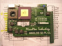
Performer-Genesis-00.JPG

Assuming the clock doubling formulas (phase lock looped?) of U7 are present in the PALs of this 68020 accelerator would be running at 1.5x the Plus" baseline clock you would indeed have a 12MHz system. Performer for Plus has 5x GAL16, this one has only 3x PA16, wo wondering about that?

Delete SE and Classis connector provisions from Performer and you would have the basic, if munged around a bit, plan form of this simple 12MHz system board.
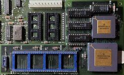
12MHz Accelerator c75 Rotated.jpg
__________________________________________

Been wondering about that PSU/Chassis. Does that sit under or over the FDD?
- If low power, it could be a hard drive assembly mod?
- seems very odd geometry with curious lack of connection points
- what's on the end poof that Red/Black wiring bundle?
- If powerful enough to run the Plus that fan's oddball positioning could be cooling a hotter flyback on a VidCard/Monitor board?
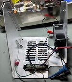
12MHz Accelerator PSU-c.jpg

That's a lot of jumper wire, test clip leads for anything stock, no?

The only other things that screams "PROTYPE" to me at all would be the wire wrapping on the jumper header pins near U4, that's a semi permanent- much more reliable, durable bodge replacing a simple header connection and the empty SIP connector at S1.
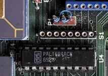
12MHz Accelerator - Jumper.jpeg


edit: dunno, all this would be habitual, over the top flights of fancy for the sake of discussion. ;)
 
Last edited:
The only other things that screams "PROTYPE" to me at all would be the wire wrapping on the jumper header pins near U4
For what it's worth, I just opened an old hard drive assembly and found that they (PLI) had wirewrapped the wires on the HDD itself that go to the SCSI selector dial on the back (which was soldered normally), so I guess some stuff from that era was still being wirewrapped in production units of things.

I also was curious about the SIP connector, is a resistor pack missing? Or does it just serve as test points?
 
That doesn't stop the Performer from running at 16MHz sans crystal. The difference between Classic and SE versions of Performer are the GAL at U7 next to the SE PDS slot with what became the standardized 16MHz reference clock in its pinout.

Maybe I'm not understanding your logic, but the plus (and I'm pretty sure the SE and Classic too) uses a 16mhz crystal and halves it for the cpu. The performer can just use the raw clock for 16Mhz no?

For this to run at 12Mhz would require a 1.3 clock divider to be implemented on those pals, and it seems unlikely...
 
Yep on 16MHz clock halving done on the Compacts* ** logic boards to generate the 8MHz CPUCLK.

But nope, that'd require a bodge to tap the 16MHz clock line at source somewhere on the Plus logic board on installation.
That would radically violate the KISS principle. ;)

Plus predated C16M on the SE PDS, having only the halved 8MHz CPUCLK available on the 68000 socket. Hence, the clock doubling GAL that's not necessary on the SE/PDS variant. Dunno for sure about Performer/Classic, but I'd bet that GAL at U7's required on its 68000 socket/pin leg interface as well.

1.5x crankup of 8MHz CPUCLK input seems reasonably simple? Whatcha thinkin'@Bolle


* SE/30 is a limited expansion Macintosh IIcx in Compact Mac case, setting up the precedent for crappy displays on AIO Macs.
** Color Compact is a Micro AIO with crappy display (resolution) that's in no way a Compact Mac!😜
 
Last edited:
1.5x crankup of 8MHz CPUCLK input seems reasonably simple? Whatcha thinkin'@Bolle
You can't do a non-integer multiple in a PLD in a practical manner. Achieving a 2x clock in pure logic requires enough shenanigans that I wouldn't see apple going for even on a prototype.

Therefore it's running at the original CPU clock.

I agree with lobust's hypothesis. It just serves as a way to have an accessible 68020 CPU development platform. Performance is not essential. Unfortunately, the missing ROMs are likely required for it to work.
 
I agree with lobust's hypothesis. It just serves as a way to have an accessible 68020 CPU development platform. Performance is not essential. Unfortunately, the missing ROMs are likely required for it to work.
That makes a lot of sense in the context of my Folklore read, But why 12MHz parts, if indeed they were such as seemingly marked? Was an 8MHz 68020/FPU combo ever even released?
You can't do a non-integer multiple in a PLD in a practical manner. Achieving a 2x clock in pure logic requires enough shenanigans that I wouldn't see apple going for even on a prototype.
That's what I was wondering about, makes a lot of sense. I tke it thad downshifting from 16MHz to 8MHz is more easily done in logic? Is it done in a far more simple method?
 
That makes a lot of sense in the context of my Folklore read, But why 12MHz parts, if indeed they were such as seemingly marked? Was an 8MHz 68020/FPU combo ever even released?

That's what I was wondering about, makes a lot of sense. I tke it thad downshifting from 16MHz to 8MHz is more easily done in logic? Is it done in a far more simple method?
Yeah, you can manage power of two divisors very easily - dividing by two is just single a flip-flop/register.

It is likely 12mhz were simply the first 68020 parts made and/or sampled out for engineering.
 
Back
Top