• Hello MLAers! We've re-enabled auto-approval for accounts. If you are still waiting on account approval, please check this thread for more information.

IIsiSuperMacPDSadapterRAMhack™

Trash80toHP_Mini

NIGHT STALKER
68040
TopicMorph alert! Original thread title:

KnuckleDraggin'HardwareHacker™ vs. EuroDIN Connector . . .

. . . acting as stubborn as the hack3r happens to be = }:)

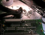
Electrical components and connectors should NEVER piss off a lunatic who thinks of the 22 oz. Estwing Rip Claw Framing Hammer hangin' off his tool belt as the smallest useful variety of (upholstery tack hammers don't count [;)] ]'> ) that particular tool category . . .

Odds are he's got a friggin' Nail Nipper in one of the pockets of said tool belt and a bit less than the amount of patience with which most electronics hackers must have been blessed . . .
knuckledraggerdoom2p.jpg

What friggin' EuroDIN Connector? :?:

Elegant it ain't, but hanging the Hemostat off the naked, fat end, of the stubborn pins . . .

. . . and re-applying the solder sucker from above might be considered a bit more civilized . . . }:)

Muahahahahahahahahahahaaaaaaaaaaaaaaaaaaaaaaaaaaaaa!!!!!!!!!!!!!!!!!!!!!!!!!!!!!!!!!!!!!!! :lol:

 
No worries, the card's fine! :approve:

I'd already desoldered the vast majority of the pins, but a few refused to submit to the solder sucker iron. }:)

It's a simple passthru PDS adapter for the IIsi made by SuperMac for their Video Cards. What got me interested enough to buy a pair of them was the intriguing provision of those unpopulated thru-holes for SIPs.

My (novice electron pusher's) working theory (WAG) would be that they used zener diode packs in those locations during the development process. We used discrete components on the ISA card for the interface cable on the ROM/Font Emulator project back in that same day.They dampen noise on address/data and signal lines by dumping anything over the spec'd voltage to ground, which is pin one on each row. I think they (or for whatever the holes were really intended) were deemed unnecessary in the production run.

Those SIP pads make a VERY handy wedge point for a hack of the IIsi/SE/30 PDS! }:)

The card makes an even handier chassis for a series of hacks for said PDS. :approve:

MemoryMaximificationHack™ . . . which would be my particular use. No pesky RAM on my IIsi MoBo! }:)

2nd PDS slot hack . . . I don't need this, but it'd come in handy for conventional IIsl multicard use

Additional uses for the SE/30 crowd:

_____Side Saddle version of the 2nd PDS Card Adapter hack. (at a much lower point than those on gamba)

_____Development chassis for a PowerCache IIci PDS adapter

_____Top or side Saddle PassThru Implementations are a possibility

Overall, it will be a lot of hacking fun and it could turn out to be quite useful . . . [:D] ]'>

 
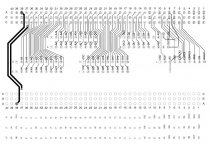
First results of the hardware hackin' wedge's verification:

iisisupermacramhack007x.jpg.dfb61e589152d09054353b06f1621405.jpg


Sorry about the faint lines on the .jpg export, I'll post a better one later. edit: Done!

The essentials of the hack, assuming my assumptions are correct, is to hijack all the Bank Select and Row Address Select Lines from the IIsi's Memory controller.

Meanwhile, I'll be disabling the pitiful 1 MB Bank soldered to the MoBo.

Essentially, I'm testing the waters for doing a REVERSE SIMM Saver Hack, replacing all the IIsi's 30 pin SIMMs and said 1 MB Bank with 72 pin SIMM Module(s?) in sockets mounted on a daughtercard PCB that PiggyBacks onto DIP sockets mounted in the unimplemented (zener diode?) SIP thruholes on this SuperMac IIsi PDS Adapter.

Next step is to buzz all the connections again to verify the layout.

Then, or concurrently, I need to do an overlay layer with the pin locations and signals tapped by all those lovely SIP pads!

Then the fun begins, PCB Layout & Prototype Playtime! }:)

 
Ummm, the RAM control lines aren't available in the PDS slot. I kind of missed that detail in the PM a while back. Didn't make the jump that you're grabbing your signals from the PDS slot. Or are you? Perhaps you're just using the PDS card as a convenient circuit board?

Anyway, you may want to think of the computer as a hierarchy of busses. The PDS slot provides access to the CPU bus. But the RAM control signals are behind the memory controller. The CPU bus is on one side of the memory controller and the RAM signals/bus are on the other side of the memory controller.

The Data lines should be common though, but sometimes there are buffers so that the memory controller can detach the RAM portion of the data bus from the rest of the data bus. Buffers are used to split a bus into two, so that separate action can take place in the two segments, or so that stray signals on one segment won't interfere with activity on the other segment.

I would start out by tracing the data lines on the logic board. Get the pinout of the 68030 and an ohmmeter and trace the data signals to see if they lead directly to the SIMM pins, or if there are buffers in between. I would bet that there must be, at least on Bank A, because the video circuitry is supposed to be able to access Bank A while the CPU is accessing bank B and the only way that can happen is if there are some buffers to isolate the two chunks of data bus from each other.

So the data bus will be fairly simple, but that built-in video may be a problem. And you can probably get access to the data bus in the PDS slot.

The address lines are multiplexed to the RAM though. And the memory controller provides refresh signals through the /RAS and /CAS signals. So you really need to steal the memory controller signals (RAM address, /RAS, /CAS, /WE) somewhere between (inclusive) the memory controller and the SIMM sockets/soldered down memory.

 
Thanks for the info!

I figured anything I need from the memory controller I'll patch, hopefully with some kind of shielded wire. I'll be trying to keep all the signal, data bus, address bus and patched memory controller lines exactly the same length.

I'll have the 32 data lines, 32 addressing lines, plus power & ground from the PDS, leaving just four lines remaining to patch to the Daughtercard on the PDS Adapter Cards "sockets" from the memory controller . . .

. . . unless that multiplexing scheme rears its ugly head and bites me onna' @$$!!!!. :-/

I've got a SIMM Saver Card for the "reversing" of the design. It makes four 30 pin SIMMs compatible with a 72 pin SIMM socket. It's a very simple funnel array, so I'm fairly sure I shouldn't have any trouble turning the tables on the design.

LOTS of research to do on both SIMM types, the memory controller signals . . . and now buffering! ::)

Expect LOTS of questions from me as I go about this hack, trag! :approve:

It's a lot of fun tackling a memory card hack again after 20 some years! [:D] ]'>

 
It's morning and my brain is almost back online again . . . xx(

. . . maybe just a bit more than it was last night anyway!

I wasn't thinking there'd be the same fast side/slow side bus issues on an unbridged '030 PDS that there are on the 2300c's PBX bridged '030 PDS.

The early Duos used L2 Cache in the DuoDock over the Docking Connector/'030 PDS, so I was assuming that there'd be no problem putting main memory on an unbridged '030 PDS expansion card . . .

. . . oh well . . . if it were easy . . . sane people might try doin' crazy crap like this! 8-o

So it's back to the DevNotes and block diagrams I go!

THX again! ;)

 
Here's a pic the signals that are readily available . . .

. . . on the unimplemented SIP thru-holes on the SuperMac PDS Adapter.

iisiramhackinterface009.jpg.3cc14608397fad94ad689abf6bc4686a.jpg


All these signal connections have been double checked/buzzed and certified . . .

. . . haven't done more than a rudimentary count of Data & Address lines yet, but they're all there! :approve:

The rest remain Sanskrit for the time being . . . ::)

 
iisisupermacramhack010.jpg.12ea904b98ee6bde48117e83e5def258.jpg


I can do a better 1080p ScreenShot to convert than I can export as a .jpg straight from Illustrator . . .

. . . go figure! ::)

Only the PDS Lines unimplemented on the SIP pads remain on the top view.

+5V will be jumpered to one of the unused DIP Pads or through the hole, if necessary.

If I can get it researched well enough to lay out & prototype the PCB, the Memory Signals will be transmitted from the Memory Controller on a DIP Pin/Ribbon cable connector to the ProtoCard.

I was amazed that this method of posting on ImageShack worked at all . . . like I said . . . go figure!

.PDF of the state of the hack.

 
I've got no idea at all! :beige:

At this point, I'm most interested in seeing if Bank 1's being filled to capacity makes any difference! :?:

Will this allow for an increase in Vampire Video's Color Depth a/o allow for larger screen resolutions when the OS is installed "for ANY Macintosh," as it usually is when running a Rocket under RocketShare?

With a 33 or 40 MHz 68040 on board, considering the dearth of multi-threaded apps in my footlocker, the IIsi's '030 isn't going to be doing much of anything except acting as an I/O Controller and Video Card for the Rocket in the NuBus Adapter.

Worst case scenario, is that nothing comes of this memory hack at all . . . :-/

. . . aside from obvious educational benefits, creative outlet . . . :o)

. . . keepin' the cobwebs outta' the ole' noggin' for a bit longer . . . :approve:

. . . and yet more Post Grad Credits in the School of Hard Knocks! ::)

In that case I'll just use the IIsi MoBo to drive the Macintosh Portrait Display sitting on top of the IIsi in 8 bit grayscale on the left side of the workstation. The Radius Color Pivot II VidCard under the MoBo will drive my 19" ViewSonic LCD at 8 bit 16" resolution sitting in the middle of the workstation. Right side'll be either the LC 475 w/fitted 12" RGB or maybe that'll be on the IIsi and . . .

. . . whatever, the combinations are legion! :lol:

 
The soldered over thru-holes on this card may be very useful for the original purpose!

I got some sporadic flakiness using it "as is" (FlatCardStackConnectorHack™ aside) with the Radius Color Pivot II/IIsi card. Adding the 10bT card might cause more noise, so zeners mounted on the modded SuperMac PDS Adapter might wind up being just what the EE ordered!

 
Well, I've pulled my head out of the DevNotes and GttMFH2E so here goes!

. . . sometimes there are buffers so that the memory controller can detach the RAM portion of the data bus from the rest of the data bus. Buffers are used to split a bus into two, so that separate action can take place in the two segments, or so that stray signals on one segment won't interfere with activity on the other segment.
I would start out by tracing the data lines on the logic board. Get the pinout of the 68030 and an ohmmeter and trace the data signals to see if they lead directly to the SIMM pins, or if there are buffers in between. I would bet that there must be, at least on Bank A, because the video circuitry is supposed to be able to access Bank A while the CPU is accessing bank B and the only way that can happen is if there are some buffers to isolate the two chunks of data bus from each other.

So the data bus will be fairly simple, but that built-in video may be a problem. And you can probably get access to the data bus in the PDS slot.
From reading the docs on the IIfx, IIci and the IIsi, it seems that the only buffering is on Bank A. Bank A is a four SIMM array on the IIfx and IIci, but a pathetic 1 MB of SMT RAM ICs on the lowly IIsi.

Bank A is buffered for access as video memory on the IIci and the IIsi for the rudimentary Vampire Video hardware configured as a Pseudo Slot at address 00.

The IIfx, lacking this circuitry or buffering, still shows "Mac II Video" at Pseudo Slot 00, which I find very interesting.

If I'm reading the information on RAM access times of the IIci and the IIsi correctly, the video buffering on bank A has absolutely no effect on access times if there is no monitor (probably detected by polling the sense lines during initial setup of the machines at boot) using the Vampire Video Circuitry.

Therefore I surmise that I can likely ignore the buffering of Bank A on the IIsi, so long as no monitor is hooked up to Video Out on the MoBo.

Desoldering (or cutting the chip select a/o power traces to) the I MB of Bank A Mobo Ram and installing the equivalent of a maxed Bank A like the four SIMM Slots available on the IIci ought to be a possibility.

I haven't figured out the logistics of the hack as yet, I think I'll wait for some comments before proceeding. ;)

Comments? :?: PLEASE!!! :o)

 
It's looking like hacking (multiplexed) System Memory onto this card is out of the picture for the nonce, but that WAG about translating the DuoDock's Cache implementation into a IIsi Cache Adaptation over the 030 PDS Slot has been confirmed. Props to beachycove for findingthat lil' gem. Macintosh IIci VS IIsi

Du'Oh, though! :I The IIsi L2 Cache prospect is pretty much obvious in hindsight. That's what the PDS is designed to do, get the Processor's Direct Signalling (per trag, see above) onto an expansion connector. Otherwise the PowerCache Cards wouldn't work, nor the FPU sockets.

L2 Cache SRAM ought to be right at home on the raw 68030 signals as well. Now I'm a very happy camper . . . erm . . . hacker! [:D] ]'>

p.s. hacking L2 onto the NuBus adapter or the RCPII/IIsi Card could be another avenue of approach as well, but . . .

 
I checked out the IIci Cache Card as my first line of inquiry and decided that puppy was waaay past figuring out, as expected. I remembered there was a big honking ASIC mounted dead center, but was surprised to see two different types of SRAM . . . WTH(eck) is "Tag SRAM," WTH does it do and W(ho)TH cares?

Whatever . . . the big honking ASIC's name is: NMC CONTROLLER, but its function is readily apparent . . .

. . . some sort of black magic having to do with cache cards . . . DUH!!

Checked out the DevNote specs for the DuoDock, no L2 Cache, drat! The ICs that I recalled were VRAM. The L2 Cache is in the Dock II and the Dock+ but I have a working Dock+ on hand to test it out. I finally found the DevNote for the DuoDock II . . . this appears to be about as complicated as I was figuring it might wind up being. FEH!

I didn't remember any specialized ASIC on my Dock+ board that might be for controlling Cache and I was right . . . Apple rolled the Cache Controller into the JET Video Controller along with the SWIM . . . %^!$@#%$#$^%!!!!!!!!

Maybe it's a lot more simple than the IIci Cache implementation . . . at least there's none of that freakin' TAG SRAM in the Spec! ::)

Does anyone remember seeing any documentation for adding Cache to the 68030? :?:

 
Yep, thought of that, but I was thinking more along the lines of getting it to work within the Mac OS. Not sure if it'll just use it if it's there or what.

TattleTech lists the presence of cache in its reports, so the OS checks for it on startup, if my read on the workings of TattleTech is anywhere in the general vicinity of how it works. I'm assuming it runs the equivalent of the POST check/whatchamacallit.

 
Back
Top