I actually did spend a little bit of time figuring out those table entries back when I was looking at the Flasher app! I named them, btw; the names weren't anywhere in the code. I didn't inspect the code in depth, but I at least figured out the table entries. Here they are, along with some random comments from my disassembly:
View attachment 102628
View attachment 102629
Both entries support two gestalt machine IDs: gestaltPowerBook500 (72) and another unknown ID of 73. They use $20000000 as the address for ROM reads and $20400000 as the address for ROM writes, but they differ a bit after that point.
PB500SIMM1 looks for four Intel 28F020 chips across the 32-bit data bus, but there are two banks, so it has 8 total chips, with only 4 activated at a time. Each chip is 256 KB, so four of them is 1 MB (that's the $100000 line) and there are 2 banks (that's the 2 below it) so the total ROM size is 2 MB. It should show up as "Blackbird Flash" in the Flasher UI if detected.
PB500SIMM2 looks for four Intel 28F008SA chips. This time there is only one bank. Each chip is 1 MB, so four of them is 4 MB (that's the $400000 line), so I think this would be a 4 MB module in total. It uses a custom erase and programming function that's different from the other table entries. I haven't looked deeper into the code or datasheets, but I'm guessing the 28F008SA needs different erase/write algorithms than the other chips and that's why. Its Flasher UI name is "Malcolm Flash".
The enable programming function shared by both of them writes $00000000 to address $20400000 and then waits 16 ms (I think). The disable programming function writes $00000000 to address $20000000 and does the same wait. Those are the same addresses used for writing and reading the data, so I'm not sure if the first write to $20400000 is what unlocks writes and writing to $20000000 locks them again, or what.



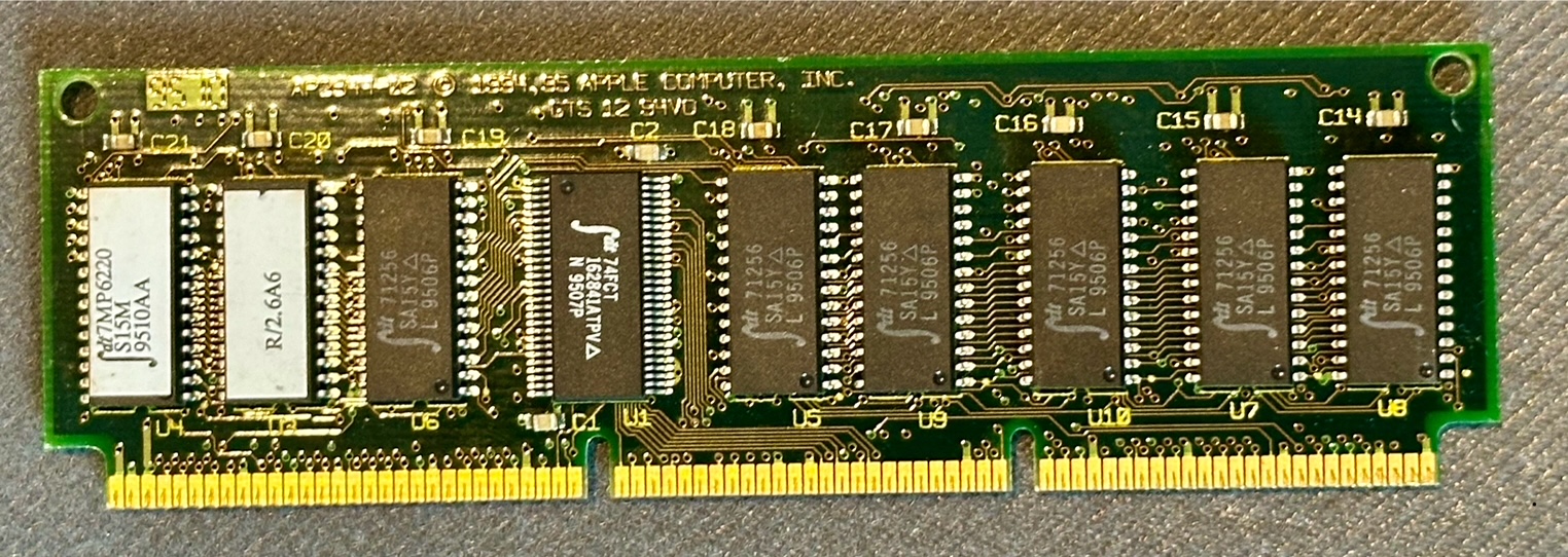
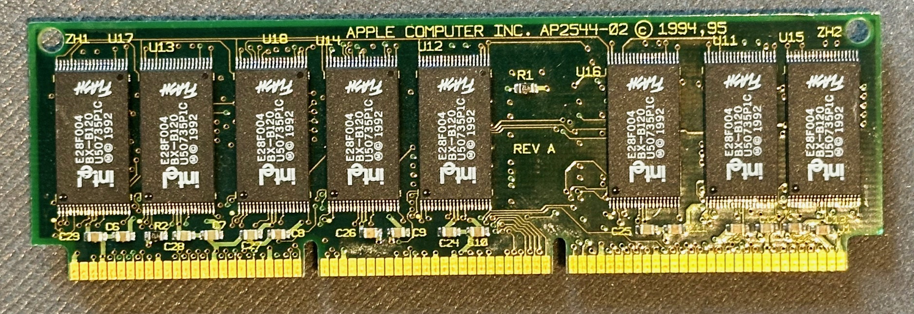

 . Might all have been scrapped, but you never know.
 . I'm pretty sure the flasher tool can reprogram also this card with an appropriate adapter.




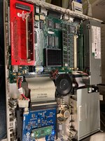
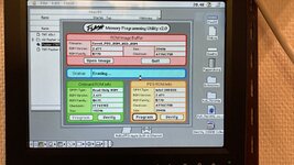
 ). I did also test it in an LC3, but it did not get detected by the machine, so I'd say anything older than LC475 is a no go.
 I'm so glad you were able to verify it with the STB ROM SIMM. It makes sense because the table entries showed that combination as being supported.