Trash80toHP_Mini
NIGHT STALKER
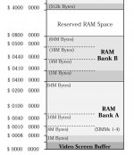
This is the Memory Map of the IIsi from the Developer Note:

The space at the end of Bank B between $ 0800 0000 and $4000 0000 is just sitting there waiting to be hacked!
GttMFH2e doesn't break the map of the SE/30 down, but lists it as $ 0000 0000 to $ 4000 0000 which is the same as the 128MB mapped to Banks A & B of the IIsi and the Reserved RAM Space combined. What size block does that reserved range define?
I've given up on trying to expand the memory of the IIsi by connecting it to Bank B, nothing seems to work out but a huge ball of patch wires. I've figured out how to combine the ancient IC stacking method and Pin Jumper methods so that I'll only have to patch A10 and A11 from MDU, but that's a side issue.
The /RAS line quirkiness is what got me going.
View attachment 22710
View attachment 22711
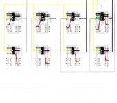
The two banks of the IIsi (hoping it's the same for the SE/30) each use only two of the four /RAS lines available on MDU. I went ahead and blocked /RAS1 & /RAS2 into my 72pin SIMM adapter Schematic to illustrate what I'm asking. Bank A is full to the brim between $ 0000 0000 and $ 0400 0000. The next block is the 64MB of Bank B, but that lovely Reserved RAM Space lurks above.
If I go ahead with the SIMMspender adaptation of Bank B, might jumpering Bank A's /RAS0 and /RAS3 from MDU to a 128MB 72pin SIMM on the adapter open up the Reserve? Looks to me like the two independent address and control line sets on MDU, each using different pairs of /RAS lines might be interpreted as the makings of a Four Bank memory system when the /RAS lines are mixed and matched?
I'm thinking along the lines of a double Banked 128MB SIMM for "Bank B". One 64 MB Bank would be addressed as IIsi or SE/30 Bank B in the usual manner by /RAS1 and /RAS2. With the second 64MB Bank on the 128MB SIMM sharing the remainder of Bank B's signals, might /RAS0 and /RAS3 open up the possibility of third Bank implementation? Dunno if it'd be C or D, but the Map's open for it.
Got no clue, just noticed some loose ends which piqued my curiosity. Thought I'd mention the WAG I made on how they might be tied together . . . or not.
But I'll pose the question before looking at how Bank C and Bank D are implemented in my Quadra 950, if that's what they're called.
The memory preserve is there, if we build it, could a /RAS line hack bring it home? :blink:
edit: I'm not expecting that Bank to magically appear, something like Connectix Virtual might be able to squeeze the extra bits out of an oversized, double stuffer SIMM?
Last edited by a moderator:

