• Updated 2023-07-12: Hello, Guest! Welcome back, and be sure to check out this follow-up post about our outage a week or so ago.

SE/30 DiiMO accelerator cloning

Melkhior

Well-known member
@mdeverhart Is it really necessary to _slow_ the signals? From the Atmel's datasheet for the G16V8, there's already a bit of variability there.
SymbolParameterMin (-10)Max(-10)Min (-15)Max (-15)Units
tPDInput or Feedback to
Non-Registered Output
8 outputs switching
310315ns
XC9536XL in speed grade -10 will match the fastest of the two G16V8 speed grade, and will be at least as fast or faster on almost every parameters (/OE to output enable/disable being the exception, you need to go one speed grade better as the CPLD is 11ns vs. the GAL 10ns).
I _think_ (but with not a lot of confidence) that the one thing that matters is for the logic to be 'fast enough' to reach its destination in time. Being faster than the original should not be a problem.
I attach some automated conversion of @Bolle 's GAL code from the first post; 'u*.v' are the trivial translations, 'u*_opt.v' has been filtered to do some DeMorgan, double negation elimination, and 2-ary->n-ary conversion to be more readable. Very untested, there could be bugs in my quick'n'dirty translator.
 

Attachments

  • se30diimo_gal_in_verilog.zip
    11.2 KB · Views: 5

zigzagjoe

Well-known member
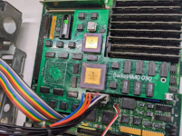
Something new, based on @Bolle 's hard work.

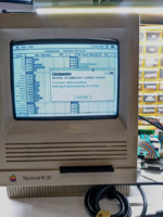
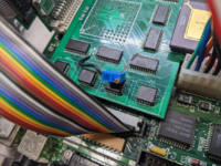
The cache isn't working, but the fact that this even bonged had me hooting and hollering (scared the cat!). Ignore how filthy the board is... it is freshly assembled and I couldn't resist trying it out before cleaning.

1685508529708.png
1685509477518.png
 

zigzagjoe

Well-known member
In case anyone has interest in this, here's some working files I've made to assist my own efforts to understand the GAL logic. I wrote a script to replace the variable names in the dumped sources with pin names from Bolle's schematic in order to aid in understanding the GALs. Next steps for me is understand exactly what the control panel tickles to turn the cache on and see if I can't find the corresponding state in the GALs to probe for.

I did find an interesting inconsistency - The U7 raw dump has a slight difference from result of running the dump through JED2EQN and EQN2JED. A single fuse is different. I don't know enough about the GAL format to manually determine if it is significant or not (yet). Didn't make a change in my cache not working, though.

Other notes.... I'm not sure why MicroMac decided to run the FPU at half speed (25mhz), I put a jumper to run it at 50mhz which seems to work just fine (as far as speedometer is concerned) with a more or less linear performance improvement.
 

Attachments

  • DiiMO GAL work files.zip
    59.2 KB · Views: 3

zigzagjoe

Well-known member
I have identified how the cache is turned on and off in the control panel. Disassembly of all the code resources turned up these two functions - this looks exactly like what I'd expect to poke a magic address in order to turn cache on/off. Macsbug confirms that lowest bit changes as expected when toggling the cache on/off, so this is definitely it. Next question is how does the hardware recognize / implement this.... more to come...

Code:
ROM:0000069A turnOnCache?:
ROM:0000069A                 moveq   #1,d0            
ROM:0000069C                 _SwapMMUMode                ; enter 32 bit mode with D0=1
ROM:0000069E                 move.b  ($50F01F03).l,d1     ; read a byte from magic addr
ROM:000006A4                 ori.b   #1,d1                ; set bit 1
ROM:000006A8                 move.b  d1,($50F01F03).l    ; write value back
ROM:000006AE                 _SwapMMUMode
ROM:000006B0                 rts

ROM:000006B2 turnOffCache?:
ROM:000006B2                 moveq   #1,d0
ROM:000006B4                 _SwapMMUMode                ; enter 32 bit mode with D0=1
ROM:000006B6                 move.b  ($50F01F03).l,d1    ; read a byte from magic addr
ROM:000006BC                 andi.b  #$FE,d1            ; clear bit 1
ROM:000006C0                 move.b  d1,($50F01F03).l    ; write it back
ROM:000006C6                 _SwapMMUMode
ROM:000006C8                 rts

Expect data in D31 - D24 because its a byte xfer. See 7-23 in docs
Looks to me like this is acting like a register. Maybe it goes to SRAM somehow?

Magic address $50F01F03
Bits set         Which GALs have this bit
----------------------------
A30 = 1        1,7
A28 = 1        1
A23 = 1        none
A22 = 1        none    
A21 = 1        none
A20 = 1        none
A12 = 1        none
A11 = 1        10
A10 = 1        10
 A9 = 1        10
 A8 = 1        6
 A1 = 1        7
 A0 = 1        7
 

Melkhior

Well-known member
Looks to me like this is acting like a register. Maybe it goes to SRAM somehow?
I doubt there's spare space in the SRAM beyond the cache data themselves (data, tags, valid bits typically). It's more likely the GALs (or PAL) are decoding addresses to match for this one and then storing internally the bit(s) in one of the registered GALs.

In U1, N28 is a good candidate for matching the I/O space ($5xxxxxxx). You have it as:
Code:
/o_N__28 = /i_BA31 * f_BA28 * /f_BA29 * /i_BA30
with
Code:
i_BA31=2 /i_BA30=11 f_BA29=13 f_BA28=14
in the GAL header.
But there's no inversion anywhere in the HW for BA30, so I suspect the negation (/) is just part of the name in there and this is testing for A31 low, A30 high, A29 low and A28 high, so $5 in the upper nibble.

N__28 is then combined with more address lines to produce N__11 and N__34 in U10. N__34 is used in what appear to be the reset function in U6, while N__11 is used extensively in U4. As U4 is a registered GAL with NC pins that are heavily used in the equations, I would assume at first that U4 is the one with configuration/status bits.
 

zigzagjoe

Well-known member
I doubt there's spare space in the SRAM beyond the cache data themselves (data, tags, valid bits typically). It's more likely the GALs (or PAL) are decoding addresses to match for this one and then storing internally the bit(s) in one of the registered GALs.

In U1, N28 is a good candidate for matching the I/O space ($5xxxxxxx). You have it as:
Code:
/o_N__28 = /i_BA31 * f_BA28 * /f_BA29 * /i_BA30
with
Code:
i_BA31=2 /i_BA30=11 f_BA29=13 f_BA28=14
in the GAL header.
But there's no inversion anywhere in the HW for BA30, so I suspect the negation (/) is just part of the name in there and this is testing for A31 low, A30 high, A29 low and A28 high, so $5 in the upper nibble.

N__28 is then combined with more address lines to produce N__11 and N__34 in U10. N__34 is used in what appear to be the reset function in U6, while N__11 is used extensively in U4. As U4 is a registered GAL with NC pins that are heavily used in the equations, I would assume at first that U4 is the one with configuration/status bits.
Agreed on the SRAM. It is weird though, because this memory location acts like a normal 8 bit register which is not what I'd expect of a bare minimum implementation inside GAL(s). I'd expect some bits to not be settable/readable. If we assume GALs are doing this, there's still the question of BD0 goes into U6, where are the other data bits coming/going?

Never mind, answered part of the memory - this addressed location belongs to someone else. Without the Diimo, I still get the "C1" default value out of it. Toggle cache in control panel, it writes C0. The region spans from 50f01e00 - 50f01fff and seems to be a single byte. It's ticklish, I get some interesting crashes playing with other bits. My takeaway, the original device doesn't care about bit 0, so diimo just borrows this as a handy location to poke bits at.

Oddly, I thought it should look at B24 not B0 given we're doing byte accesses, but I suspect it's just my ignorance of the 68030's bus sizing stuff. I last got into the nuts and bolts of a 68008 with a SBC design some years back, so we've come just a little ways since :)

AFAIK inversions in the definitions are operative - the log files from compiling the GAL code backs this up. So for some reason BA30 is an active low input.... this could be an optimization from when these were originally designed, or perhaps a compiler trick. With the inversion in the code, that cancels out anyways.
 

Melkhior

Well-known member
Never mind, answered part of the memory - this addressed location belongs to someone else. Without the Diimo, I still get the "C1" default value out of it. Toggle cache in control panel, it writes C0. The region spans from 50f01e00 - 50f01fff and seems to be a single byte. It's ticklish, I get some interesting crashes playing with other bits. My takeaway, the original device doesn't care about bit 0, so diimo just borrows this as a handy location to poke bits at.
Given how much I've stared at those addresses, I should have noticed it straightaway. They're I/O address documented in HardwareEqu.a from the Rom. $50F00000 is VIA1. $50F02000 is VIA2. AFAICT, the 16 registers from the W65C22 are mapped one every $200, so the range you quote is vBufA from VIA1 in HardwareEqu.a, which is
Code:
ORA/IRA Output Register "A" Input Register "A"
. OR* are described as:
When a line is programmed as an output, it is controlled by a corresponding bit in the Output Register (ORA & ORB). A
Logic 1 in the ORA or ORB will cause the corresponding output line to go high, while a Logic 0 will cause the line to go
low. Under program control, data is written into the ORA or ORB bit positions corresponding to the output lines which
have been programmed as outputs. Should data be written into bit positions corresponding to lines which have been
programmed as input, the output lines will be unaffected.
If I understand the schematic correctly, that particular bit is unused as the line associated to it (PA0) is only connected to the edge debug connector. So it is effectively a free storage bit. It seems PA1 and PA2 are also unused, so changing the 3 low-order bits should be "safe". The other 5 are actually used, so those might have some major side-effects if you poke at them behind the system back.

I suspect the value is never read, and the GALs are capturing the write to this location on-the-fly to get the 1-bit value.
 

Phipli

Well-known member
Given how much I've stared at those addresses, I should have noticed it straightaway. They're I/O address documented in HardwareEqu.a from the Rom. $50F00000 is VIA1. $50F02000 is VIA2. AFAICT, the 16 registers from the W65C22 are mapped one every $200, so the range you quote is vBufA from VIA1 in HardwareEqu.a, which is
Code:
ORA/IRA Output Register "A" Input Register "A"
. OR* are described as:

If I understand the schematic correctly, that particular bit is unused as the line associated to it (PA0) is only connected to the edge debug connector. So it is effectively a free storage bit. It seems PA1 and PA2 are also unused, so changing the 3 low-order bits should be "safe". The other 5 are actually used, so those might have some major side-effects if you poke at them behind the system back.

I suspect the value is never read, and the GALs are capturing the write to this location on-the-fly to get the 1-bit value.
Interesting, and the fact that it is broken out to the edge connector means that they can monitor it for debugging easily. I mean, you could stick an LED on it!
 

zigzagjoe

Well-known member
Given how much I've stared at those addresses, I should have noticed it straightaway. They're I/O address documented in HardwareEqu.a from the Rom. $50F00000 is VIA1. $50F02000 is VIA2. AFAICT, the 16 registers from the W65C22 are mapped one every $200, so the range you quote is vBufA from VIA1 in HardwareEqu.a, which is
Code:
ORA/IRA Output Register "A" Input Register "A"
. OR* are described as:

If I understand the schematic correctly, that particular bit is unused as the line associated to it (PA0) is only connected to the edge debug connector. So it is effectively a free storage bit. It seems PA1 and PA2 are also unused, so changing the 3 low-order bits should be "safe". The other 5 are actually used, so those might have some major side-effects if you poke at them behind the system back.

I suspect the value is never read, and the GALs are capturing the write to this location on-the-fly to get the 1-bit value.
Aha. Makes sense. Yes, changing the upper bits has interesting effects. A variety of crashes, mainly. I agree the GALs must just be capturing the write.

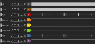
I'm starting to poke around with a logic analyzer... tag_reset seems to stay low, that'd be at least part of the problem. I'll have to dig further
1685900386037.png
 

zigzagjoe

Well-known member
Aha. Makes sense. Yes, changing the upper bits has interesting effects. A variety of crashes, mainly. I agree the GALs must just be capturing the write.

I'm starting to poke around with a logic analyzer... tag_reset seems to stay low, that'd be at least part of the problem. I'll have to dig further
View attachment 57595
Looking at this closer, I think f_I_TAG_RESET is our guy. An output on U6 that is stateful as it is self-referential and also uses BD0. And it looks like i_I_RESET should be able to clear it, though I haven't quite figured out how it would clear its state short of i_I_RESET being asserted. While I haven't looked for documentation, given that the control panel immediately clears that bit if cache is disabled, it suggests the original has that capability. Probably just need to stare at it more, but I'm going to probe the f_I_TAG_RESET input signals first.

I've attached a CSV file (as .txt) that lists all the signals going into the GALs with the signal names off the schematic, with the types of pins it gives clarity as to which GAL outputs a signal and which simply use it. I haven't 100% validated it, I used some code to generate it similar to the one I used to mogrify the variables into something legible.

Code:
f_I_TAG_RESET = i_I_RESET * f_I_DSACK0 * f_I_TAG_RESET
    + /i_I_AS_PDS * i_BD0 * /f_I_DSACK0 * i_BA8 * /f_RI_W * i_N__34
    + i_I_AS_PDS * i_I_RESET * f_I_TAG_RESET
    + i_I_RESET * f_I_TAG_RESET * f_RI_W
    + i_I_RESET * f_I_TAG_RESET * /i_N__34
    + i_I_RESET * f_I_TAG_RESET * /i_BA8
f_I_TAG_RESET.oe = vcc

chasing N_28 and N_34
Code:
(U1)
/o_N__28 = /i_BA31 * f_BA28 * /f_BA29 * /i_BA30

(U10)
/o_N__34 = f_BA9 * i_BA11 * f_BA10 * /i_BA16 * /i_BA14 * /f_BA17 * /i_BA13 * /f_N__28

working through these bits and BA8 from  TAG_RESET, I get the following. Definitely looks like a winner so far....
         | 3322 2222 2222 1111 1111 11
 HEX     | 1098 7654 3210 9876 5432 1098 7654 3210
------------------------------------------------------------
           0101 xxxx xxxx xx00 x00x 1111 xxxx xxxx 
50f01f03   0101 0000 1111 0000 0001 1111 0000 0011
 

Attachments

  • GAL_PINS.txt
    9.9 KB · Views: 2

zigzagjoe

Well-known member
Pity we can't edit posts on this.... Yes, Diimo supports live toggle of cache. f_I_TAG_RESET is the cache enable/disable. Which is also PA0 on VIA1 and goes to top pin 5 on the debug connector, so as @Phipli mentioned that's a nice easy debug trick.

My issue with f_I_TAG_RESET turned out to be BA17 on U10 didn't get soldered, so N$34 never was asserted to allow enable cache. I must have gotten sloppy with the paste. Fixing that got me to instant crash territory when cache turned on, which turned out to be my having cut f_TAG_U28_IO_4 trace while drag soldering. After that - yes! The cache is working! At 30mhz, anyways.

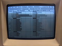
40mhz and 50mhz instantly lock when enabling cache, and I haven't completely validated stability at 30mhz yet. It does feel noticeably snappier, and benchmarks at least the same or faster than running at 50mhz without cache. I've got a couple of random crashes though which make me think it's not 100% stable. A/UX works with cache on and it runs a lot better over stock, 5 minute boot is down to 2 already. A/UX is a big part of why I wanted to clone an 030 accelerator (also the form factor), so it's nice to validate this.

1685942234553.png
left - 30mhz CPU & FPU, cache working
right - 50mhz CPU & FPU, cache not working.

From here, things will get more fiddly.... I'll probably probe around a bit more, but I may decide to spin a new board since I know I have design deficits - poor routing of traces, stupid .1mm trace width, the potential to simplify routing by tweaking the buffers, missing cutout for the power latch, etc. At least my schematic is validated.

Some hardware stuff to improve / tweak too... My TAG ram is only 15ns (instead of 12), though these are really hard to source. The ATFs are rated at 10ns, Micromac used a mix of 10ns and 7ns GALs & Bolle noted the ATFs' propagation characteristics are different too.

@Bolle, were you able to hit stable 50mhz operation on your clones?
 

zigzagjoe

Well-known member
You may want to look at IDT's application note AN-46, "A 33MHz MC68030 Zero-Wait Cache Memory", available in the "1991 STATIC RAM DATA BOOK".That includes some timing analysis that might be of interest. Edit: in particular appendix H ("50MHz MC68030 TIMING ANALYSIS").
Thanks, this is fantastic. I've been struggling a bit filling in the gap between the goal/concepts and the hardware, to understand what / why the GALs are doing.
 

Melkhior

Well-known member
@zigzagjoe Beware that the IDT doesn't implement bursting, but other manufacturers choose to implement bursting. TI has an application note ("SN74ACT2155/56 Cache Enhances MC68030 Processor Performance") to use their own chips (which do tags, comparison, and auto-incrementing of addresses for bursting) in their 1990 data book. Timing analysis is less detailed IIRC (and they don't have full listings of everything, unlike IDT), but it's still interesting and cover how bursting work. If the cache card 'intercepts' A2/A3 to the SRAM, it implements bursting (the MC68030 doesn't change A2/A3 during bursting if I've understood things correctly, so the device must do that).
 

zigzagjoe

Well-known member
A2 and A3 aren't plumbed to SRAM, and the U7 looks at those lines in conjunction with the data coming out of the 3rd TAG RAM. I haven't quite wrapped my head around what it's doing with that data, yet. Looks like validity bits to me based off the app note. U6 however is also looking at A2 and A3 with some state associated, that looks a lot like I'd think auto-increment could be implemented.

Code:
o_SRAM_A13 = i_N__18 && i_N__17 && i_BA3
    || !i_N__18 && !i_BA2 && !i_BA3
    || !i_N__18 && !i_N__17 && i_BA2 && i_BA3
    || i_N__18 && !i_N__17 && i_BA2 && !i_BA3
    || i_N__18 && !i_BA2 && i_BA3
    || !i_N__18 && i_N__17 && !i_BA3
o_SRAM_A13.oe = vcc
o_SRAM_A0 = i_N__17 && i_BA2
    || !i_N__17 && !i_BA2
o_SRAM_A0.oe = vcc

I'm going to have to do some more probing, I think measuring AS->MAT0->STERM/DSACK at high speed will give me a good picture of the end to end cache latency. Then some more high level probing to understand the overall flow.
 
Last edited:

zigzagjoe

Well-known member
It seems that my issue is the phase shift/invert clock generated in U2 that drives U2, U3, U5, U10. Taking a break from a logical approach, I was monkeying with the U2 clock and hit a case that was stable with cache on at 50mhz. The speed was incredible, and benchmark results seemed to match expectations.

Test equation was o_U2_CLK_50M =/ i_CPUCLK_50M .
However much to my confusion the phase shift clock signal was not registering in the logic analyzer, while the Mac was happily chugging away. This is due to the clock voltage dropping to something 0.7 average and a peak of 1.5v!! I'm honestly amazed that anything was working, the GALs specify a 2v minimum Vih so we were in the undefined behavior region. Functionally, I'm sure it was a radical phase shift. At least it proves the board seems to be close to being able to do 50mhz.

Original equation was /o_U2_CLK_50M = /i_CPUCLK_50M which seems to functionally invert the output signal, not due to logic but instead by propagation delay. Average output voltage of this was 1.6v which implies logic high somewhere in 3v. Not ideal, but within spec. Interesting that the test equation had so little drive strength.

I don't see abnormal resistance on the line, so I'm just assuming the ATF isn't quite up to driving this clock signal. I wish I had a scope that could do these speeds so I could have a better look at these clocks, though I can at least play with my logic analyzer's threshold voltage.

1686153968663.png

The right way to fix this would be a buffer, I think. However, I may just monkey with the equations and pull up-resistors and try to find a case where I seem to get a seemingly-healthy clock signal voltage, and functional card. The original card had these 4 GALs in close proximity to each other without clock termination. Unfortunately I split them without recognizing I'd extended that clock across the board nor did I give it the additional care I gave the system clock routing.... Not ideal.
 

zigzagjoe

Well-known member
Just talking to myself, but hopefully this is interesting to somebody.

I've been playing with the board using the low voltage clock signal that shouldn't really be working while I wait for parts. So far the only quirk I've noticed is that it does not like RAM tests while warm. Sits on the happy mac forever, and eventually gives a sped up death chime. Cold boot RAM tests don't seem to have this issue, and it is usually passes the test fine after turning it off for a minute. I'm not really worried about it, it is probably related to the gray area for that clock signal. Otherwise, the board has been (surprisingly) stable, I haven't been able to provoke any issues yet.
1686502628199.png

The clock issue is some sort of issue with the ATFs. Not sure why, but they seem to have issues driving this clock signal at that frequency even without no load on the pin. I'm using the ATF16V8B-10JU, so they should be good for faster clocks than this... but, I noticed the same behavior with two isolated ATFs off the board, so the problem isn't the board design. I've got some conventional GALs on order (faster ones, too) and I'm going to swap a few of the more sensitive ones out - U1 and U2 at least. I might end up swapping them all and recording what if any effect if any it has on performance.

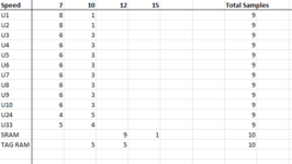
For informational purposes, I collected speed rating info from 10 pictures of boards where possible.

1686500926946.png

As far as the TAG RAM goes, given that it is always matching, as long as it is valid by the time AS.LOCAL is asserted, I'm thinking the -15 speed rating I'm using is fine. Which is good, because finding the TAGs is nearly impossible. Measuring with my logic analyzer, it's close, but the worst case I've found is an occasional tie which could just be jitter. There's other dependencies in the state machine though that I really need to start assigning some tentative names to so as to better understand the overall function.
 

Phipli

Well-known member
So far the only quirk I've noticed is that it does not like RAM tests while warm. Sits on the happy mac forever, and eventually gives a sped up death chime. Cold boot RAM tests don't seem to have this issue, and it is usually passes the test fine after turning it off for a minute.
I'm fairy sure it only does a RAM test on cold boot - it doesn’t do one after a restart.

Regards,
Someone who has booted a C650 with 260MB of RAM and almost died of boredom waiting.

:ROFLMAO:
 

zigzagjoe

Well-known member
I'm fairy sure it only does a RAM test on cold boot - it doesn’t do one after a restart.

Regards,
Someone who has booted a C650 with 260MB of RAM and almost died of boredom waiting.

:ROFLMAO:
260MB in a 68K mac? I'd believe that would take forever!

So, it doesn't do a test on reset or clean restart, but the specific Special->Shutdown then clicking restart in the "It is now safe to turn off..." dialog seems to do one. Very much an edge case...

This leads into a follow up question for someone that knows the Mac OS boot process in more detail - is there something about Mode32 or the SE/30 specifically that causes it to do a memory test at the happy mac screen? I always thought it happened earlier in the boot process.
 
Top