• Updated 2023-07-12: Hello, Guest! Welcome back, and be sure to check out this follow-up post about our outage a week or so ago.

Reverse Engineering the Macintosh SE PCB & Custom Chips for 1:1 reproduction

Trash80toHP_Mini

NIGHT STALKER
I was involved in the reverse engineering of the Amiga 500+, Rob Taylor (@PeepoUK in twitter) was the man behind that idea - he since went on to do all the models of C64 board. We've got a discord server, and after watching Adrian Black's repairathon, i realised that no one had done this for a Mac...there's no reason to not do it either, so...i volunteered :D
Your project is just amazing, following it with intensity.

Also, id love for this to be done with the SE/30. I have a pile of those boards dead and screwed from battery juice. Be forewarned, the SE/30 has traces that run in the middle layers as I saw, and I am not sure how your approach would be for that. 
Given X-Ray(?) technology capable of non-destructively testing ridiculousl complex layered CPU's and the like for tweaking production and Trojan Horse detection, I cannot imagine that a layered scan of the SE/30 or any other board could be all that problematic.


Trash80toHP_Mini

NIGHT STALKER
Your Neolithic disassembly approach is the bombe! :lol: I did that very same same thing for reverse engineering the 1400's PCMCIA/TREX daughtercard about 18 years ago! That was before I discovered the encasement in epoxy/milling machine process.


olePigeon

Well-known member
Just out of curiosity:  can the PDS slot on the SE be broken out into multiple slots like the later LC PDS slots?  On the LC, even though there's only 1 physical slot, it has address locations for up to 3 (I think) slots.


Trash80toHP_Mini

NIGHT STALKER
You have an x-ray machine handy? Yea.....  
Nope, just a link to an IEE Spectrum article on Ptychographic X-ray laminography. [:p]

There must be some service bureau type place capable of using much older X-Ray tech on a bared SE/30 board? However I much prefer your build it back up in improved form from reverse engineered schematics than the 1:1 copy approach. But by far I'm no purist here as so many are. It takes a menagerie. [;)]


Trash80toHP_Mini

NIGHT STALKER
Only ground, no power plane? That seems odd to me in a multilayer PCB. I was under the impressions that layers were the sum of bonded, two sided pairs: 2-4-6-8 etc.

Just out of curiosity:  can the PDS slot on the SE be broken out into multiple slots like the later LC PDS slots?  On the LC, even though there's only 1 physical slot, it has address locations for up to 3 (I think) slots.
LCIII PDS has more than one (maybe all three?) Interrupts/Slot IDs in its pinout, but in every case they're tagged with: Not used in the LCxx. That suggests a ROM limitation to me.

 
Last edited by a moderator:

Trash80toHP_Mini

NIGHT STALKER
Forgot to mention that LCs are Slot Manager era tech, implemented or not. SE's not a Slot Manager implementation AFAIK with no provision to handle additional cards in its architecture. Best case would be accelerators hooked up to VidCards AFAIK. Multiple slot LC expansion chassis implementations appear to be good for a combination of a couple of non-competing expansion cards or for turning cards on and off individually IIRC.

 
Last edited by a moderator:

techknight

Well-known member
I see your cut-out borders on one side, but its missing the cutout completely on the PDS side? is this intentional? just curious. 


techknight

Well-known member
Thats funny. ive seen them on both sides. Maybe different board revisions were different? 

Edit: I had to go back and look at the photos. Yea that board version has the cutouts only on one side. Strange! ive seen it on both. 

So they must have had different board versions over the years. 

 
Last edited by a moderator:

cheesestraws

Well-known member
The last SE I took to bits certainly only had them on one side, because I remember swearing about it while I was trying to get the board out...


PB145B

Well-known member
There is a 1986 and a 1988 revision. I own both, but don’t remember the notches. I’m assuming it’s the 1986 revision that has them on only one side and the 1988 revision that has them on both sides. I’d have to look at them again.


Trash80toHP_Mini

NIGHT STALKER
Thats funny. ive seen them on both sides. Maybe different board revisions were different? 
The 1988 revision jibes with development of the SE/30 which shipped January 19, 1989. SE/30's new chassis with provision for vertical PDS expansion was adopted for late SE production. Have you seen an early SE/30 with tabs on both sides? By 1988, SE upgrades were all but standard equipment, they were far larger than Apple's spec for board size and pushed the vertical limit for installation. Directions for products as early as the Radius16 specified the "pry the sides of the chassis apart method" of installation. So I wonder if they slotted the 1988 revision SE board on both sides to ease expansion, putting less compression and flexion stress on chassis and motherboard? With its vertical expansion slot, the SE/30 didn't have any pressing need for cutouts on both sides, but I'm curious if any did?
 

Michael_b

Well-known member
The 1988 revision jibes with development of the SE/30 which shipped January 19, 1989. SE/30's new chassis with provision for vertical PDS expansion was adopted for late SE production. Have you seen an early SE/30 with tabs on both sides? By 1988, SE upgrades were all but standard equipment, they were far larger than Apple's spec for board size and pushed the vertical limit for installation. Directions for products as early as the Radius16 specified the "pry the sides of the chassis apart method" of installation. So I wonder if they slotted the 1988 revision SE board on both sides to ease expansion, putting less compression and flexion stress on chassis and motherboard? With its vertical expansion slot, the SE/30 didn't have any pressing need for cutouts on both sides, but I'm curious if any did?
FWIW my SE board which came with the SE/30-style chassis has no cutout.


Kai Robinson

Well-known member
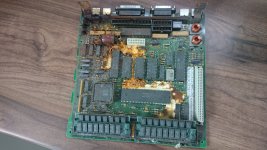
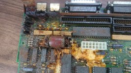
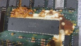
Update time! After a busy week, i got a whole Mac SE! That was well and truly buggered by the wrath of a maxell battery...

Still, the board being dead can still be very, very useful in reconstructing the ground and power planes - yes, it might look like a 2-layer board, but it is, in fact, a 4 layer board - with signals on top and bottom, and inner planes being +5v and GND. 12v is carried on surface traces 1mm wide. 

Rather than sanding the layers, i'm manually testing each via and component with a 'loose end', seeing if they belong to the +5v or GND planes, and basically trying to line them up with the charcoal imprint of a schematic that exists - seriously, if anyone has a better version of that schematic, please, for the love of al that is scientific and factual, can someone SELL IT TO ME! :D

DSC_0378.jpg

20200702_174602.jpg

20200702_174619.jpg

 
Top