• Updated 2023-07-12: Hello, Guest! Welcome back, and be sure to check out this follow-up post about our outage a week or so ago.

Radius MagicBus pinout

cheesestraws

Well-known member
Radius MagicBus was a compact version of the SE PDS used on Radius' products for the SE. It allowed Radius graphics cards to be used along with a Radius accelerator, and if you didn't have an accelerator, you could use a "jumper card" which was just an adapter.

IMG_2041.jpg

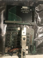
I have been unable to find the pinout for the MagicBus connector, so when @mg.man dropped off a spare jumper card, I thought I'd better buzz it out and see what the pinout looked like.

A CSV file is attached. Some consumption notes to go with it:
  • MagicBus pin numbers and row letters follow the silkscreen on the jumper card, as above.

  • Where a pin on the MagicBus connector goes to multiple pins on the SE connector which are commoned together, the "SE pin" column contains the first one I found. No pattern beyond that.

  • I checked this all twice, but if you blow up something irreplaceable, that's on you... ;-). If you use this info, please at least check that the 12V is in the right place before you plug anything in.

  • Signal names are taken from from Designing Cards and Drivers, p.264.

  • I have only done this based on the jumper card. I cannot rule out that, for example, one of the pins marked as GND in this CSV file is actually used to communicate in some way between the accelerator and the MagicBus card. YMMV.
 

Attachments

  • magicbus pinout.csv.zip
    1.9 KB · Views: 6

cheesestraws

Well-known member
The connector on the jumper card is a JAE PICL-60S-ST which unfortunately seems to be out of production: datasheet with drawings is attached here. Pin pitch is 1.27mm with 3.2mm row spacing, by the look of it; a quick look on RS suggested several possible options to mate with it, but I haven't tried any yet.
 

Attachments

  • DSAIHSC0007807.pdf
    429.5 KB · Views: 10

demik

Well-known member
Nice reverse here !

I'm wondering what sort of daughtercards existed for this MagicBus adapter
 

Trash80toHP_Mini

NIGHT STALKER
@cheesestraws Nice, thanks for the heads up! Now I can compare this to full PDS signalling:

MB Pin No,MB A/B,SE Pin,Signal name
1,A,30A,GND
2,A,6C,/DTACK
3,A,7C,/R/W
4,A,8C,/LDS
5,A,9C,/UDS
6,A,10C,/AS
7,A,12C,/RESET
8,A,14C,D0
9,A,15C,D1
10,A,16C,D2
11,A,17C,D3
12,A,18C,D4
13,A,19C,D5
14,A,20C,D6
15,A,21C,D7
16,A,22C,D8
17,A,23C,D9
18,A,24C,D10
19,A,25C,D11
20,A,26C,D12
21,A,27C,D13
22,A,28C,D14
23,A,29C,D15
24,A,19B,/IPL1
25,A,27A,E
26,A,28B,/EXT.DTK
27,A,30C,GND
28,A,30C,GND
29,A,30B,+12V
30,A,32A,+12V
1,B,30C,GND
2,B,4A,A1
3,B,5A,A2
4,B,6A,A3
5,B,7A,A4
6,B,8A,A5
7,B,9A,A6
8,B,10A,A7
9,B,11A,A8
10,B,12A,A9
11,B,13A,A10
12,B,14A,A11
13,B,15A,A12
14,B,16A,A13
15,B,17A,A14
16,B,18A,A15
17,B,19A,A16
18,B,20A,A17
19,B,21A,A18
20,B,22A,A19
21,B,23A,A20
22,B,24A,A21
23,B,25A,A22
24,B,26A,A23
25,B,28A,C8M
26,B,29A,C16M
27,B,30A,GND
28,B,13B,+5V
29,B,13B,+5V
30,B,32B,-5V

A little confused about you labeling? Can't see the attachments at work, so posted TXT. ;)

Row Pin name description output capability (high/low)
A 1 FC2 Function code 2 Output Drive: 40J..LA/.4mA, 30pF (Input) (Load: 100J..LA/100Jl.A, 50pF)
A 2 FC1 Function code 1 Output Drive: 40J..LA/.4mA, 30pF (Input) (Load: 100Jl.A/100Jl.A, 50pF)
A 3 FCO Function code 0 Output Drive: 40J..LA/.4mA, 30pF (Input) (Load: 100J..LA/100Jl.A, 50pF)
A 4-26 Al-23 Address 1-23 In/Out Load: 250J..LA/1mA, 100pF Drive: 40 J..LA/.4 mA, 30pF
A 27 E E (enable) clock Output Drive: 40J..LA/.4mA, 30pF
A 28 C8M 7.8336 MHz Output Drive: 20J..LA/.2mA, 20pF Mc68000 clock
A 29 c16M 15.6672 MHz Output Drive: 20J..LA/.2mA, 20pF gate array and IWM clock
A 30 GND Logic ground
A 31 +12V +12 volts Output Drive: 150mA total, from all +12V pins
A 32 +12V +12 volts Output (see the section "Power Budget")

B 1-9 GND Logic ground
B 10 Reserved For future Apple use; do not connect
B 11 Reserved For future Apple use; do not connect
B 12 /HALT Mc68000 Halt In/Out Load: 300 J..LA/6mA , 50pF Drive: 0~0Jl.A (Connected to /RESET, pin C-12)
B 13-17 +5V +5 volts Output Drive: 1.5 A total, from all +5V pins (see the section "Power Budget")
B 18 /IPLO Interru pt level 0 In/Out Load: 100J..LA/2mA, 50pF (VIA, SCSI.IRQ) Drive: 40J..LA/.4mA, 30pF (Open collector; 3.3K ohm pullup)
B 19 /IPL1 Interrupt level 1 In/Out Load: 1 00 JlA/2mA, 50pF (SeC) Drive: 40 JlA/.4mA, 30pF COpen collector; 3.3K ohm pullup)
B 20 /IPL2 Interrupt level 2 In/Out Load: 100JlA/2mA, 50pF CNMI switch) Drive: 40 JlA/.4mA , 30pF COpen collector; 3.3K ohm pullup)
B 21 /BERR Bus error In/Out Load: 100JlA/2mA, 50pF Drive: 40 JlA/.4mA, 30pF COpen collector; 3.3K ohm pullup)
B 22 Spare Not connected
B 23-'-27 Reserved For future Apple use; do not connect
B 28 /EXT.DTK External /DTACK Input Load: 100JlA/2mA, 50pF Ctri-states main C3.3K ohm pull up) board's /DTACK)
B 29 GND Logic ground
B 30 +12V +12 volts Output Drive: 150mA total, from all +12V pins
B 31 +12V +12 volts Output Csee the section "Power Budget")
B 32 -5V -5 volts Output Drive: 100mA

C 1 /VPA Valid periph. Output Drive: 40JlA/.4mA, 30pF address
C 2 /VMA Valid memory Output Drive: 40 JlA/.4mA , 30pF address Onput) (Load: 100JlA/100JlA., 50pF)
C 3 /BR Bus request Input Load: 1 00 JlA/2 mA , 50pF
C3.3K ohm pullup)
C 4 /BGACK Bus grant Input Load: 1 00 JlA/2 mA , 50pF acknowledge C3.3K ohm pull up)
C 5 /BG Bus grant Output Drive: 40 JlA/.4mA, 30pF e 6 /DTACK Data transfer In/Out Load: 100JlA/2mA,
____50pF acknowledge Drive: 40 JlA/.4mA, 30pF
C3.3K ohm pullup, /EXT.DTK low, tri-states main board's /DTACK)
C 7 R/W Read/write Output Drive: 40J.LA/.4mA, 30pF (Input) (Load: 200J.LA/2mA, 50pF)
C 8 /LDS Lower data Output Drive: 40~.4mA, 30pF strobe (Input) (Load: 100J..lA/1mA, 50pF)
C 9 IUDS Upper data Output Drive: 40~.4mA, 30pF strobe (Input) (Load: 100J..lA/1mA, 50pF)
C 10 /AS Address strobe Output Drive: 40~.4mA, 30pF (Input) (Load: 200JlA/3.2mA, 50pFj 3.3K ohm pullup)
C 11 /PMCYC Processor Output Drive: 40J.LA/.4mA, 30pF memory cycle (High during video access to RAM)
C 12 /RESET System reset In/Out Load: 300JlA/6mA, 50pF Drive: 40J.LA/.4mA, 30pF (Open collectorj 1K ohm pullup)
____(Connected to /HALT, pin B-12) C 13 +5V +5 volts Output Drive: 1. 5A total, from all +5V pins (see the section "Power Budget")
C 14-29 DO-15 Data bus, In/Out Load: 250JlA/1mA, 100pF bits 0-15 Drive: 40J.LA/.4mA, 30pF
C 30 GND Logic ground
C 31 Spare Not connected
C 32 -12V -12 volts Output Drive: 100mA

MagicBus is dedicated to Radius FPD and TPD for the SE and so only needed to support single bit graphics. Comparing it to full PDS will be interesting indeed! :)
 
Last edited:

Trash80toHP_Mini

NIGHT STALKER
I've added MagicBus prefix to the PDS pinout file above on paper. So I know what's missing and needs to be added to expand the bus to full PDS spec.Gotta get that info into the file and sort out formatting.

Intention is to have the thruholes present for an either/or choice in populating the board. Header socket rows will work for my FPD/TPD Card connector interface if we don't come up with a suitable mating connector.

DIMM socket cut down to length looks like a good option for installing a PDS prototyping board within the TPD form factor. But that's for another thread, only documenting the differentiation in this one.That seems to be on point?
 

Trash80toHP_Mini

NIGHT STALKER
This looks like everything that's on the PDS, but missing from MagicBus:

U - A1 - FC2 Function code 2 Output Drive: 40J..LA/.4mA, 30pF (Input) (Load: 100J..LA/100Jl.A, 50pF)
U - A2 - FC1 Function code 1 Output Drive: 40J..LA/.4mA, 30pF (Input) (Load: 100Jl.A/100Jl.A, 50pF)
U - A3 - FCO Function code 0 Output Drive: 40J..LA/.4mA, 30pF (Input) (Load: 100J..LA/100Jl.A, 50pF)
U - A31 - +12V +12 volts Output Drive: 150mA total, from all +12V pinsU - B 1-9 - GND Logic ground
U - B12 - /HALT Mc68000 Halt In/Out Load: 300 J..LA/6mA , 50pF Drive: 0~0Jl.A (Connected to /RESET, pin C-12)

U - B18 - /IPLO Interru pt level 0 In/Out Load: 100J..LA/2mA, 50pF (VIA, SCSI.IRQ) Drive: 40J..LA/.4mA, 30pF (Open collector; 3.3K ohm pullup)
U - B20 /IPL2 Interrupt level 2 In/Out Load: 100JlA/2mA, 50pF CNMI switch) Drive: 40 JlA/.4mA , 30pF COpen collector; 3.3K ohm pullup)
U - B21 /BERR Bus error In/Out Load: 100JlA/2mA, 50pF Drive: 40 JlA/.4mA, 30pF COpen collector; 3.3K ohm pullup)
U - B29 - GND Logic ground
U - B31 +12V +12 volts Output C see the section "Power Budget")

U - C1 - /VPA Valid periph. Output Drive: 40JlA/.4mA, 30pF address
U - C2 - /VMA Valid memory Output Drive: 40 JlA/.4mA , 30pF address Onput) (Load: 100JlA/100JlA., 50pF)
U - C3 - /BR Bus request Input Load: 1 00 JlA/2 mA , 50pFC3.3K ohm pullup)
U - C4 - /BGACK Bus grant Input Load: 1 00 JlA/2 mA , 50pF acknowledge C3.3K ohm pull up)
U - C5 - /BG Bus grant Output Drive: 40 JlA/.4mA, 30pF e
U - C11 - /PMCYC Processor Output Drive: 40J.LA/.4mA, 30pF memory cycle (High during video access to RAM)
U - C13 - +5V +5 volts Output Drive: 1. 5A total, from all +5V pins (see the section "Power Budget")
U - C32 -12V -12 volts Output Drive: 100mA

Only 18 active lines to be added to flesh it out to full PDS spec!

Spares, Reserved, NC, etc. Spare 5V and GND lines likely advisable?

U - B15 - +5V
U - B16 - +5
U - B17 - +5V
U - B5 - GND
U - B6 - GND
U - B7 - GND
U - B8 - GND
U - B9 - GND
U - B10 - Reserved For future Apple use; do not connect
U - B 11 - Reserved For future Apple use; do not connect
U - B22 Spare Not connected
U - B23-'-27 RESERVED For future Apple use; do not connect
U - B24 - RESERVED
U - B25 - RESERVED
U - B26 - RESERVED
U - B27 - RESERVED
U - C31 - Spare Not connected

U = Unimplemented on MagicBus
 

Trash80toHP_Mini

NIGHT STALKER
The connector on the jumper card is a JAE PICL-60S-ST which unfortunately seems to be out of production: datasheet with drawings is attached here. Pin pitch is 1.27mm with 3.2mm row spacing, by the look of it; a quick look on RS suggested several possible options to mate with it, but I haven't tried any yet.
Have you got linkage to that RS source or any of the connectors you're considering? It looks like the pitch of a DDR2 DIMM Slot matches and half of that part might be a physical/pin compatible alternate for full PDS implementation?
 

cheesestraws

Well-known member
Have you got linkage to that RS source or any of the connectors you're considering

Not off the top of my head.

It looks like the pitch of a DDR2 DIMM Slot matches and half of that part might be a physical/pin compatible alternate.

Perhaps, but the original is quite short and also a pin header. I'm not sure what your purpose is here, but you might just be better off creating an alternate PDS type affair rather than going via magicbus.
 

Trash80toHP_Mini

NIGHT STALKER
I've been thinking header sockets of the right pitch would do nicely as your connector replacement if you can't find a suitable part?. There's enough room for running the two rows of sockets parallel to the OEM thruhole pattern as (bodged) alternative.

MagicBus-Chassis-Alignment.JPG

In that config you'd only need spacers to mate with the OEM bracket.

MagicBus-TPD-Interface-Assembly.JPG

Dunno if there's enough vertical play in the mounting slots for height matching header socket/header to mate FPD/TPD with the OEM bracket, but a printed version will be necessary at any rate. Few FPD/TPD cards I've seen on eBay have that metal bracket included.

Thought you might be interested in seeing my alternate plan of attack for connector interface? Have you looked at the missing PDS signals on MagicBus? Very curious about what's required and what's not for a video only setup, Was surprised to see full Address and Data lines implemented on a single bit VidCard. But that would be necessary for video buffer memory mapping I'd think?

Thinking I'd go from two layers to four given trace spacing required. I'll start a new thread about extending the bus, but I'd like my MicroMac Performer build to include MagicBus FPD/TPD Card compatibility along with full PDS support for DCaD playtime.
 

Trash80toHP_Mini

NIGHT STALKER
@cheesestraws Looks to me like two rows of 1.27 pitch header sockets set parallel to J2A ought to suffice for a KISS MagicBus connector bodge? Maybe not?

Not sure, I nave some some 2x5 double row sockets with that pitch which line up legs-to-sockets on J2A, but I can't get it to seat on a TPD card's pins. Could be the double row/wrong row spacing interference thing? But I have a sneaking suspicion that the pins on the OEM part don't match that header/socket spec for thickness?

And, of course, I can't find the matching headers for Digiper readings! 🙄
 
Last edited:
Top