• Updated 2023-07-12: Hello, Guest! Welcome back, and be sure to check out this follow-up post about our outage a week or so ago.

Please help me figure out what the deal is with this IIx RAM

tattar8

Well-known member
I'm trying to upgrade my IIx past 8MB of RAM.  The issue is that none of the RAM I've tried seems to be accepted.  I know the PAL is needed, and SIMMs with less than 8 chips are also no dice.  I got four SIMMs similar to the ones here: https://www.ebay.com/itm/8MB-30-Pin-SIMM-for-Quadra-950-10726-0001/312574140050 (there are two PALs visible on each chip), and four similar to the ones here: https://www.ebay.com/itm/2x-2MB-30-Pin-70ns-FPM-Memory-SIMMs-4MB-Matched-Set-Vintage-Apple-Macintosh/142837813376 , but still just got the chimes of death when inserted into Bank A, and the IIx just pretended like they weren't there if I inserted them into Bank B.  When the IIx gives the chimes of death, it is with major error code E if using the stock ROM (so data bus failure) or major code 11 if using a ROM-inator II (error sizing memory). 

Oddly enough, in both cases I can use the diagnostic mode to read and write bytes from memory addresses well into the 16MB range, so it doesn't seem as though the RAM isn't working. Writing to any address is mirrored to the same address with bit 24 flipped.  This would imply that that line is stuck at 1 or 0, but if I probe with a logic probe it I see it flashing high briefly at power-on, and A(24) behaves the same at the GLU pin to which it's connected.  So does anyone have any other ideas for things I should check?


chiaki

Member
im still try to figure out what exactly those special PAL memory do, i found only this information:

To have more than 8 MB of RAM in a Macintosh II or IIx, special 120 ns PAL SIMMs are required. These SIMMs incorporate PAL logic chips that overcome problems caused by the refresh logic on the Macintosh II and IIx.
also i figured out my IIx does not work with 1MB SIMM with three ICs (2x 1Mx4 + 1x 1Mx1 for Parity)

Only with eight/nine (e.g. 1Mx1 DRAM)


Bolle

Well-known member
Not all SIMMs that have a PAL/GAL on them are made with the II and IIx in mind.

Especially on SIMMs with a lot of chips like you linked above the PALs are used to switch between multiple memory chips based on the SIMM addressing.

They don't have anything to do with the additional refresh logic that is needed for the II and IIx.

The problem on the II and IIx is that the high density chips that are used on nearly all 4MB and 16MB SIMMs did not exist when the machines were designed.

On the Mac II(x) they used /CAS-before-/RAS-refresh. For 1M chips that existed back then the state of the write enable signal did not matter so the main CPU R/W signal was just hooked up to the SIMMs.

This allowed for DRAM refresh to happen while the CPU was doing something else like writing to a peripheral device for example.

For 4M and 16M DRAM chips the write enable signal was not "don't care" anymore for refresh cycles but instead had to be held high. Most of those ICs will end up in a test mode when a /CAS-before-/RAS refresh is triggered while the /W line is low and that's what happening here.

You can put a PAL/GAL on the SIMM itself to detect whenever a refresh is happening and set up the /W signal to the DRAM ICs accordingly (i.e into high state)

Actually nothing too fancy...


chiaki

Member
(relevant information from Apple Developer Technical Support April 1992 Document)

4 Mbit DRAMs in Revolt
When the Macintosh II was originally designed, Apple engineers intended for it to accept large
amounts of memory in the form of 4 MB and 16 MB DRAM SIMMs. That was in 1986, when 1
Mbit DRAM was difficult to find and the higher-density chips did not yet exist. The engineers
anticipated the pinouts of the yet to be introduced 4 MB SIMMs and provided all the necessary
hardware and address multiplexing to allow installation of these parts when they became available.
Woe that Cupertino is not Camelot, James Brown is still on probation, and 4 MB SIMMs do not
work as advertised in most cases. This is the story of the Revolt of the 4 MB DRAM SIMMs.
Preliminary Notes
Before diving into the problem with 4 Mbit DRAMs, there is some preliminary ground that must be
covered.
First, there are a couple ways to construct a 4 MB SIMM. Using old technology, it is possible to
cram together 32 DRAM ICs of 1M x 1 density. Using new technology, it only takes eight 4M x 1
ICs, resulting in a much smaller, lower-power module. If a 4 MB SIMM is of the large, so-called
composite type (that is, it is constructed of 32 1 Mbit ICs), then everything is fine except on the
original Macintosh II. Please refer to page 7 of this Tech Note for more information on Macintosh
II RAM.
With the FDHD SuperDrive upgrade kit installed, the Macintosh II is on equal footing with the
Macintosh IIx. That is, SIMMs made exclusively of the new 4 Mbit ICs still won’t work,
regardless of whether you are using a Macintosh II or IIx; therefore, for the remainder of this
discussion, Macintosh II is used to refer to not only the original Macintosh II, but also the IIx.
Subsequent Macintosh models have revised ROMs that recognize 4 MB SIMMs.
The 4 Mbit Problem
DRAM ICs are now available in 4 Mbit density, but they come with a very nasty surprise. JEDEC,
the committee overseeing the standardization of new solid-state devices, has added an additional
built-in test mode to high-density DRAMs. The test mode is invoked by a sequence of electrical
signals that was ignored by earlier-generation DRAM. The crux of the situation is this: under
certain conditions, the Macintosh II unwittingly activates this new test mode and large amounts of
memory become very forgetful.
More Specifically . . .
Those who are interested in the specific phenomenon occurring within the memory ICs should
consult the detailed technical data supplied by the DRAM manufacturers. This Note only explains
how the Macintosh II offends this new feature of the 4 Mbit DRAM, and hence, what might be
done to work around the problem.
The Macintosh II uses /CAS-before-/RAS refresh cycles to keep RAM up to date on its contents.
For 1 Mbit DRAM, the state of the /W control line is ignored during this type of refresh cycle. No
longer. DRAM of the 4 Mbit variety goes off into test mode if /W is asserted (low, so that the
RAM thinks it is write-enabled) during a /CAS-before-/RAS refresh cycle. The problem with the
Macintosh II is that /W is the same signal as the MPU R/W line, and if the MPU is writing to an
I/O address or a NuBus™ card concurrently with a refresh cycle, all the conditions are right for a
waltz into test mode. Unfortunately, this condition is not all that unusual, since video card accesses
qualify

Consolation for SIMM manufacturers: SIMMs constructed with an on-board PAL are not
necessarily Macintosh II-specific. SIMMs constructed in this manner should work without
modification in any usage calling for 4 MB SIMMs (except in the unlikely event that the new test
mode is required).
The Salvage Process
All is not necessarily lost, and although the situation is ugly, there is still a way to use 4 Mbit
DRAM ICs to construct 4 MB SIMMs that work in the Macintosh II. A solution lies in the addition
of a ninth IC to the SIMM. Programmed with suitable logic, a high-speed (-D or -E suffix) PAL on
the SIMM itself can recognize and intercept /CAS-before-/RAS refresh cycles and set /W
appropriately before any damage is done. More or less, the PAL becomes an intelligent buffer
between the MPU read/write line and the DRAM write-enable lines. When the PAL senses a
refresh cycle commencing, it holds /W high, ensuring that the ICs are not corrupted by the
potentially dangerous processor-generated R/W signal.
What’s the Point?
You have overcome all the problems discussed in this section and have working 4 Mbit SIMMs
installed in your Macintosh. You probably have at least 20 MB of RAM. What can you do with all
of it? Create lots of huge 32-bit PICTs and edit them all simultaneously? Model and animate Bay
Area weather patterns in Mathematica™? Yes! But, you have to use the appropriate system software
to address this memory. Also, if you’re running in 32-bit addressing mode, the applications that
you desire to use need to be 32-bit clean. For more information on 32-bit cleanliness and
addressing, please see Technical Notes #212 and #213.
Under System 7.0, applications can finally access additional physical memory over and above 8
MB. As mentioned previously in this Tech Note, the 32-bit addressing mode of System 7 requires
either a Macintosh with 32-bit clean ROMs (listing is on page 2), or else the 32-bit software
solution provided by the MODE32 system extension. A/UX is an alternative that can use up to
256K of RAM on Macintosh computers that support A/UX. Many manufacturers of large SIMMs
also offer RAM disks. This is a volatile form of storage, but can certainly be useful for I/O
intensive operations.
Other Permutations
The problem with 4 Mbit DRAM is not limited to 4 MB SIMMs. It is the 4 Mbit density of the
individual RAM ICs that causes problems with certain machines. There exist 1 MB SIMMs
constructed of only two 1M x 4 (4 Mbit) ICs. These do not work in a Macintosh II or IIx, any
more than 4 MB SIMMs constructed of eight 4M x 1 ICs.
A few machines, namely the Macintosh Plus, Macintosh SE, and Macintosh Classic, depend on
video accesses to refresh all of their DRAM. As the video circuitry accesses sequential locations
through the video frame buffer, it simultaneously refreshes row after row of memory, eventually
refreshing all 512 rows. Memory at the 4 Mbit density, however, is arranged as 1024 rows and
there are not sufficient video accesses to refresh all 1024 rows. Chunks of memory simply go
blank. Thus for a different reason, 4 Mbit DRAM parts are also not compatible with these older
Macintosh hardware designs.
Executive Summary
Owners of the Macintosh Plus, SE, Classic, II, or IIx are all likely to have problems with any 1MB SIMM carrying only two ICs, or any 4 MB SIMM carrying only 8 ICs. Any SIMM constructed in one of these ways likely uses 4 Mbit density DRAM ICs and does not account for
problems with the 4 Mbit test mode nor the video refresh strategy of older Macintosh designs.

 
Last edited by a moderator:

trag

Well-known member
So how does a PAL detect /CAS before /RAS?   I guess it could just set a register when it detects a /RAS, and reset it when /CAS comes along.   If a /CAS happens and the register isn't set, that's a /CAS before /RAS.    But I'd worry that there might be some unmatched operation somewhere.   The PAL doesn't have any concept of how much time there is between signals.  

Can we depend on there never being any stray /RAS signals?   They'll always have been part of a Read/Write operation or a Refresh?

 
Last edited by a moderator:

chiaki

Member
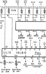
The IIcx (and SE30 too?) looks very similiar to the IIx schematics and have an PAL which control the Bank A/B RW-Line.

Maybe its possible to modify the IIx with an custom logicarray to do the same.

Clipboard02.jpg

 
Last edited by a moderator:

Bolle

Well-known member
I’ll get my II out of storage tomorrow and examine one of the SIMMs to see how it’s done exactly.

One could implement the logic into the logicboard but I’d rather not cut up traces and wire in a GAL for something as trivial as a RAM upgrade.


Bolle

Well-known member
The PAL doesn't have any concept of how much time there is between signals. 
You can use dirty tricks to measure timing intervals with PALs and GALs to some extent but I don’t think that’s needed here.


Unknown_K

Well-known member
Needing PAL RAM sucks. I have Daystar adapters for both the Mac II and IIx so being stuck with 8MB of RAM on an 040 is not ideal.


tattar8

Well-known member
Theoretically, would it be possible to design a board that hooked straight to the address and data lines (perhaps by hijacking the FPU or ROM socket) and had all the memory muxing and refresh logic onboard, allowing use of any standard SIMMs, essentially bypassing the ones on the board?


Bolle

Well-known member
Those are the SIMMs I got with eight 1k*4 DRAM chips:

IMG_3365.jpg

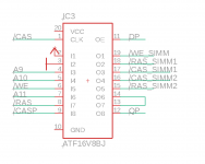
Pinout for the GAL:

Bildschirmfoto 2020-06-16 um 14.36.29.png

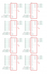
Because there are 4 data lines per chip the GAL also controls selection of the correct "bank" to select which one of the four pairs of chips is addressed depending of the state of A10 for the row and column addresses.

Bildschirmfoto 2020-06-16 um 14.47.11.png

Code:
; JED2EQN -- JEDEC file to Boolean Equations disassembler (Version V063)
; Copyright (c) National Semiconductor Corporation 1990-1993
; Disassembled from PALSIMM.jed. Date: 6-16-120
;$GALMODE MEDIUM

chip PALSIMM GAL16V8A

i1=1 i2=2 i3=3 i4=4 i5=5 i6=6 i8=8 GND=10 /nc11=11 o12=12 o13=13 
o14=14 f15=15 f16=16 f17=17 f18=18 o19=19 VCC=20 

@ues 8c323282b22c92ca
@ptd unused

equations

/o19 = /f18 * /i6 * /i8		/W will get enabled whenever either /RAS_SIMM is active and /WE is active and /RAS is active
    + /i6 * /f15 * /i8
o19.oe = vcc

//RAS_SIMM1:
/f18 = i2 * i1 * /i3 * f18 * /i5 * f15 * /i8			/CAS high * /RAS_SIMM1 high * A10 low * /RAS_SIMM2 high * /RAS low ->read/write cycle row0
    + /f18 * /i8						/RAS_SIMM1 low * /RAS low					->stay low as long as /RAS is low
    + /i1 * f18 * f15 * /i8					/CAS low * /RAS_SIMM1 high * /RAS_SIMM2 high * /RAS low		->/CAS before /RAS refresh
    + i1 * i3 * f18 * f15 * /i8					never happens because i3 always low
    + /i2 * i1 * /i3 * f18 * /i4 * f15 * /i8			never happens because i2 always high
f18.oe = vcc

//CAS_SIMM1:
/f17 = i2 * /i1 * f17 * i5 * f16 * /i8				/CAS low * /CAS_SIMM1 high * A10 high * /RAS_SIMM2 high * /RAS low ->read/write cycle column0	
    + /i1 * /f17						->stay low as long as /CAS is low
    + /i1 * f17 * f16 * i8					->/CAS before /RAS refresh
    + /i2 * /i1 * i4 * f17 * f16 * /i8				never happens because i2 always high
f17.oe = vcc

//CAS_SIMM2:
/f16 = i2 * /i1 * f17 * /i5 * f16 * /i8				->read/write cycle column1
    + /i1 * /f16						->stay low as long as /CAS is low
    + /i1 * f17 * f16 * i8					->/CAS before /RAS refresh
    + /i2 * /i1 * /i4 * f17 * f16 * /i8				never happens because i2 always high
f16.oe = vcc

//RAS_SIMM2:
/f15 = i2 * i1 * /i3 * f18 * i5 * f15 * /i8			/CAS high * /RAS_SIMM1 high * A10 high * /RAS_SIMM2 high * /RAS low ->read/write cycle row1
    + /f15 * /i8						/RAS_SIMM2 low * /RAS low					->stay low as long as /RAS is low
    + /i1 * f18 * f15 * /i8					/CAS low * /RAS_SIMM1 high * /RAS_SIMM2 high * /RAS low		->/CAS before /RAS refresh
    + i1 * i3 * f18 * f15 * /i8					never happens because i3 always low
    + /i2 * i1 * /i3 * f18 * i4 * f15 * /i8			never happens because i2 always high
f15.oe = vcc
/o14 = gnd
o14.oe = gnd
/o13 = gnd
o13.oe = gnd
/o12 = gnd
o12.oe = gnd


So basically if you leave out the row/column selection it's just pushing through /RAS and /CAS signaling as it's coming in from the logicboard and intercepts the activation of /W to only go active after the actual /RAS signal to the chips went active.

This seems to be enough to keep the chips from going into test mode. According to the datasheet the hold time for /W to go into test mode is 10ns after /RAS went low.

The GAL has a 15ns propagation delay so this must be delaying /W enough to keep the chips doing a refresh instead of going into test mode.

Not a very nice design but it works fine at least in my Mac II.

 
Last edited by a moderator:

tattar8

Well-known member
So the crucial bit is only the section governing /o19?  That seems like it could be implemented by a couple of 74 series chips on a breadboard. 

Looking at the Bomarc schematics for the II, which shares the same RAM system, each bank's /W is controlled by G7, a 74F240 inverting buffer.  But both outputs are being fed the same input, and are controlled by the same OE signal, so are they really just the same signal?  If so then I can just intercept the /W signal at pin 17 and mess with it, then send it back.


Bolle

Well-known member
That should work. You will need the /RAS signal as well and make sure that your logic chip is slow enough to exceed the hold time for the test mode. So you would have to make sure what type of RAM you are using beforehand to meet the timing requirements.

The only thing that you want to make sure is that /W does not become low while you are in the setup or hold interval for the test mode of your RAM chips which depends on when /RAS is going low. Take a look at the datasheet for any 4M DRAM chip and the timing diagrams will make it obvious what you need to do.


trag

Well-known member
So basically if you leave out the row/column selection it's just pushing through /RAS and /CAS signaling as it's coming in from the logicboard and intercepts the activation of /W to only go active after the actual /RAS signal to the chips went active.

This seems to be enough to keep the chips from going into test mode. According to the datasheet the hold time for /W to go into test mode is 10ns after /RAS went low.

The GAL has a 15ns propagation delay so this must be delaying /W enough to keep the chips doing a refresh instead of going into test mode.

Not a very nice design but it works fine at least in my Mac II.


Thank you, Bolle.   Nice investigative work.  

So, with those SIMMs, with a refresh, the memory chips would see, /CAS, then /RAS and then 15ns later, /WE.  So /WE misses the 10ns hold time window after /RAS?

Whereas, during a read or write, /RAS would go active, then /CAS would go active and in similar time frame, /WE would have gone active (if needed) 15ns after /RAS, so probably well before /CAS was signaled.

Does that sound correct?


Bolle

Well-known member
Sounds perfectly correct.

I have got another set of SIMMs from the same manufacturer and they do have a GAL as well but do not work in the Mac II.

I will compare those to the ones that work someday soon. If I get lucky and the wiring on the SIMM has separate /RAS, /CAS and /W signals to the chips those could be made to work as well.

 
Last edited by a moderator:

tattar8

Well-known member
So if I understand this right, during a CAS-before-RAS refresh cycle I want to keep WE high for some brief period after RAS drops low.  So I need to determine whether or not such a cycle is occurring, and then hold WE high.  Am I right in stating that the CAS-before-RAS cycle is the only time at which CAS will drop while RAS is still high?  If so, I could just use a D latch on the CAS and RAS signals (~CAS to the E signal, and RAS to D), and a 3-input AND gate (Q, ~CAS, and RAS) (please tell me if I've made a mistake, digital logic design is not my strong suite).

 
Last edited by a moderator:
Top