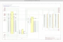
It would be very cool to have a replacement board for battery bombed systems. I just decided to give up on one today after days of debug. In all cases I've seen the custom ASICs look to be salvageable. Populating a replacement board would be much faster than going down the rabbit hole of trace repair.
-
Updated 2023-07-12: Hello, Guest! Welcome back, and be sure to check out this follow-up post about our outage a week or so ago.
You are using an out of date browser. It may not display this or other websites correctly.
You should upgrade or use an alternative browser.
You should upgrade or use an alternative browser.
Macintosh SE/30 Schematics (modernization effort)
- Thread starter Alex
- Start date
techknight
Well-known member
Dang. Too bad this wasnt done in EAGLE or I would start and roll with the PCB layout.
What do these asterisks (or are they bullets?) on the sheet labels mean? Inversion?
View attachment 33713
I didn't see this answered earlier, I apologize if I'm blind. Asterisks like that usually mean "active low". (IE, the line is pulled to zero to activate the named function. This is usually the case for chip selects. Not universally so, but usually, because TTL process chips in particular tend to float to "1" if they're left disconnected so it's the slightly safer choice.) Another common convention is to put a /slash in front of the name.
Last edited by a moderator:
Daniël
Well-known member
Another thing I'd love to see on a new board, is a separate crystal for the FPU. On the main system, I believe a lot of things are hanging on the same crystal oscillator, thus the FPU can't easily be replaced with a faster one with its own crystal to run asynchronous, which I believe should be possible if it is given its own. Would it add a lot of performance? No, but, it's the benchmark bragging rights you get, and parts and space wise I don't think a crystal, its caps and the traces should take up much space at all.
PotatoFi
Well-known member
Thank you very much for creating this schematic. I will be using it extensively over the next few days to troubleshoot a sound issue on my SE/30! The Apple schematic was readable, but working through the blur of it added an extra layer to the cognitive challenge of buzzing traces.
Trash80toHP_Mini
NIGHT STALKER
Unbelievable work! Have you thought of making a fully connected, single scrolling page by melding your individual pages?
elemenoh
Well-known member
@Trash80toHP_MiniThere should be a single file version in the folder called "Macintosh SE/30 Schematic Redraw of 050-0253-01 May-25-2020.pdf"
https://drive.google.com/drive/folders/1a29ekZRdQKhGU77sb_dueorzq3sbFU0k?usp=sharing
Please let me know if you don't see it there.
https://drive.google.com/drive/folders/1a29ekZRdQKhGU77sb_dueorzq3sbFU0k?usp=sharing
Please let me know if you don't see it there.
Last edited by a moderator:
Trash80toHP_Mini
NIGHT STALKER
Yep, saw that one and it too is fab. I was thinking about a side to side scrolling single page with connections continuous across what are now discrete pages with tagged connections. That's what I did on paper using prints of the IIsi schematic. I could trace my way across the folded map, following traces from section to section from one end to the other.
If you can't do it easily in your PCB package, I can probably do it from your PDF pages in Illustrator, or someone else might pick up the gauntlet?
If you can't do it easily in your PCB package, I can probably do it from your PDF pages in Illustrator, or someone else might pick up the gauntlet?
elemenoh
Well-known member
@Trash80toHP_Mini The KiCAD files are also posted. Please feel free to make one mega sheet with them!
Trash80toHP_Mini
NIGHT STALKER
Are the postscript paths and text exported into the PDFs from KiCAD or are they mere bitmap exports. If the former it's a piece of cake for me in AI, if the latter I may still be able to do it, but what a PITA!
johnklos
Well-known member
The last time I bought SIMMs, I bought half a dozen 128 meg SIMMs for around $10 apiece. Two were used in a Cobalt Raq, and four are waiting for when I recap a Quadra 800 motherboard so I can have a system with 520 megs.Haven't looked at 128MB as my target machines are IIsi and Quadra 950 which have discrete 64MB banks along with the SE/30's pair of such banks. IIRC, the last I looked I could get a pair of 64MB SIMMs for less than a single 128MB SIMM, has that changed?
The price difference should be negligible, but I was thinking that requiring less SIMM sockets should reduce complexity and cost, no?
Trash80toHP_Mini
NIGHT STALKER
Dunno, but I think it might be a bit more power efficient to use the 128MB variety? I lost PMs in progress twice to @trag about this stuff. I think I'm just going to start a parallel thread about the move to 72-pin in a relatively stock SE/30replacement board. I have a single, angled 72-pin Socket. I think more headroom might be necessary for the SE/30 case than the straight up variety might require?
Not to rain on your parade, but IIRC no Quadra could address more than 256MB? But maybe they can! Given original "supported" configs at time of release and the introduction of higher capacity modules using higher density RAM ICs, you never know until you try. [ ]
]
Not to rain on your parade, but IIRC no Quadra could address more than 256MB? But maybe they can! Given original "supported" configs at time of release and the introduction of higher capacity modules using higher density RAM ICs, you never know until you try. [
Trash80toHP_Mini
NIGHT STALKER
Done: 72-pin SIMM injection for updated SE/30 Schematic?
Alex, I've got your schematic PDFs loaded on the thumb drive I use to transfer files to the QS'02 Graphics WorkStation. If they open in AI9 we'll see about the scroll. [ ]
]
Alex, I've got your schematic PDFs loaded on the thumb drive I use to transfer files to the QS'02 Graphics WorkStation. If they open in AI9 we'll see about the scroll. [
Trash80toHP_Mini
NIGHT STALKER
The paths open up in AI9, but the nice type devolves into simple paths. This is doable, below is only a screen shot. Components and connectors on yours are missing, bitmap overlays? line weights and colors are easily fixed. Which pages line up in what order to left and right of this page?

View attachment 33986
Three layers showing control signals on one layer with data and address buses on the other two for viewing individually might be helpful?

View attachment 33986
Three layers showing control signals on one layer with data and address buses on the other two for viewing individually might be helpful?
Trash80toHP_Mini
NIGHT STALKER
Unfortunately, the pages don't appear to line up from one to the next in mural format as is the case of the BOMARC IIsi schematic? I'll try to figure out which ones might form a partial, but much larger picture.
Trash80toHP_Mini
NIGHT STALKER
Memory banks on p.3 are marked as Bank 0 and Bank 1. Very convenient that. : Can anyone confirm that Bank 1 on the schematic would be Bank B in the real world? Or is it Bank A for some unknown reason?
aeberbach
Well-known member
@elemenoh I just took a good look at these sheets, this is fantastic work. Now you've done the hard work of reading those fuzzy old schematics and people have had a chance to review them, a move to a working schematic in KiCad or similar is so much easier. And from there a PCB. I wonder if Apple would shut it down? There are lots of re-done Amiga PCBs around but Commodore is long gone.
IlikeTech
Well-known member
I really doubt that they care about these machines at all, much less go after someone recreating the PCBs. It's been done for the Apple II machines, so I doubt they would start now! No worries!I wonder if Apple would shut it down? There are lots of re-done Amiga PCBs around but Commodore is long gone.
quorten
Well-known member
Wow, really nice work @elemenoh, this is just what I was hoping to see happen sometime.
Definitely I'd like to see these schematics make their way into a better information repository than Google Drive, like the 68kMLA wiki, etc. I'd offer that probably the best way to go about maintaining/improving the schematics would be to put them in a GitHub repo or anything more proper of a revision control system than Google Drive.
Sounds like @Bolle may have started on laying out the footprints as a first step in creating the printed circuit board layout. Even without complete PCB traces, this would allow for the creation of an "interactive BOM" which can be helpful for guiding a recap operation, for example.
For sure, it would be interesting to see this go further and include other Macintosh models too. As I'm also familiar with KiCad, I'd also be willing to chip in to the PCB design.
Similar threads
- Replies
- 96
- Views
- 11K
- Replies
- 504
- Views
- 77K
- Replies
- 19
- Views
- 2K
- Replies
- 125
- Views
- 11K
