• Updated 2023-07-12: Hello, Guest! Welcome back, and be sure to check out this follow-up post about our outage a week or so ago.

Asynchronous 68882, error 11

Melkhior

Well-known member
Hello all,

I've built for my IIsi a new PDS adapter with a 68882 FPU socket, PLCC version. I got myself a PLCC 68882 rated for 33 MHz from what I believe to be a reputable vendor on eBay.
My design includes an external 32 MHz oscillator (MXO45HS-3C-32M0000, couldn't find 33 MHz one in stock), and a small manual switch that drives a 74LVC1G3157 silicon switch so that the FPU clock comes from either the system clock or the on-board oscillator. I subsequently discovered that @Siliconinsider has a similar design for the Classic II, minus the silicon switch - as far as I can tell the clock goes through the jumper. Easier & cheaper & known to work, wish I had done the same, but oh well...

When I try it in my IIsi:
  • Set to system clock, TattleTech sees the FPU and Speedometer 4.02 produces FPU results as expected (slightly better than a SE/30).
  • Set to my own oscillator, TattleTech sees the FPU, and Speedometer insta-crash with error 11.
Anyone knows of any reason that would happen (other than the obvious, that is, I got a re-marked 68882 that's actually not rated for 33 MHz) ? Could I have screwed the clock design? Not enough decoupling capacitance for 32 MHz operation ? (I have something like over 32 uF near the FPU and another 10-something on the other side of the board near the oscillator, no sure how much is used in @Siliconinsider design). Something else?

I should solder myself a second adapter with a 25 MHz oscillator (slowest I have in stock), but soldering another set of 192 pins is not something I look forward to :) (120 for the motherboard-side connector, 68 for the socket, 4 for the oscillator... I didn't solder the second 120-pins connector yet as I don't have a PDS card to test it with anyway).
 

Nixontheknight

Well-known member
Hello all,

I've built for my IIsi a new PDS adapter with a 68882 FPU socket, PLCC version. I got myself a PLCC 68882 rated for 33 MHz from what I believe to be a reputable vendor on eBay.
My design includes an external 32 MHz oscillator (MXO45HS-3C-32M0000, couldn't find 33 MHz one in stock), and a small manual switch that drives a 74LVC1G3157 silicon switch so that the FPU clock comes from either the system clock or the on-board oscillator. I subsequently discovered that @Sili[/[/B]B]coninsider has a similar design for the Classic II, minus the silicon switch - as far as I can tell the clock goes through the jumper. Easier & cheaper & known to work, wish I had done the same, but oh well...

When I try it in my IIsi:


      • Set to system clock, TattleTech sees the FPU and Speedometer 4.02 produces FPU results as expected (slightly better than a SE/30).
      • Set to my own oscillator, TattleTech sees the FPU, and Speedometer insta-crash with error 11.
Anyone knows of any reason that would happen (other than the obvious, that is, I got a re-marked 68882 that's actually not rated for 33 MHz) ? Could I have screwed the clock design? Not enough decoupling capacitance for 32 MHz operation ? (I have something like over 32 uF near the FPU and another 10-something on the other side of the board near the oscillator, no sure how much is used in @Sili[/[/B]B]coninsider design). Something else?

I should solder myself a second adapter with a 25 MHz oscillator (slowest I have in stock), but soldering another set of 192 pins is not something I look forward to :) (120 for the motherboard-side connector, 68 for the socket, 4 for the oscillator... I didn't solder the second 120-pins connector yet as I don't have a PDS card to test it with anyway).

I'd say try getting a different fpu
 

Bolle

Well-known member
I don’t think you’ve got an electrical problem. I have run whole accelerators including CPU, FPU and all the support logic and SRAM without any decoupling caps at all and they’ve been fine.
I would indeed check around the silicon switch if that’s causing the problem. Can you remove it and just bodge wire the oscillator in to rule it out?
 

Melkhior

Well-known member
I don’t think you’ve got an electrical problem. I have run whole accelerators including CPU, FPU and all the support logic and SRAM without any decoupling caps at all and they’ve been fine.
OK, thanks. It seems to be a major issue for "modern" high-speed silicon, but presumably old tech in the tens of megahertz range is a lot more forgiving. That's one fewer concern.
I would indeed check around the silicon switch if that’s causing the problem. Can you remove it and just bodge wire the oscillator in to rule it out?
That's a definite possibility, but both clock signals (20 MHz from the PDS & the oscillator) are going through it, and TattleTech always sees the FPU - though I'm not sure how, but I presume it tries some FPU instructions (?) so there should be some clock going through...
Removing it my be tough, I'm not very dexterous and it's quite small (SOT-23). Maybe I can start by connecting my logic analyzer and check I have a 'reasonable' signal on both side (don't have an oscilloscope, 200 MHz logic analyzer is the best I can do).

Otherwise that particular IIsi works beautifully ;-)
 

Melkhior

Well-known member
Well, I couldn't find a good way to connect my logic analyzer as I didn't add test point. And I don't have the equipment to unsolder the switch - just a soldering iron is clearly not sufficient. Same for the oscillator.

So I fell back on the "let's solder another 192 pins" option, and did another board with a 25 MHz oscillator. And for now, it seems to work - Speedometer doesn't crash, and produce results slightly improved over the 20 MHz clock. So it seems the principle of the design is sound.

So I guess either the first board has an issue at 33 MHz (design or assembly), or the chip can't run at 32 MHz.

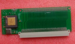
Here's what the 32 MHz board looks like:

PDS_small.jpg

Clearly it's missing an important connector :) I don't have a PDS card to test it with, so I haven't soldered the second DIN connector for now.

It's on GitHub now.
 

Bolle

Well-known member
Why the unnecessarily long clock trace from the oscillator over to the FPU?
I have found that a lot of newer 5V oscillator cans have really weak outputs. Move the FPU socket out of the way a bit and put the oscillator right next to it for minimum clock trace lengths.
Putting termination resistors towards VCC and GND at the end of the clock trace can help too.
 

Melkhior

Well-known member
Why the unnecessarily long clock trace from the oscillator over to the FPU?
The extra oscillator was kind of an afterthought; in one iteration it was much closer (above FPU, left of the manual switch), but finding available 5V oscillators in the appropriate footprint was a challenge. So I moved it to where I had some room left for a larger, more available, easier-to-hand-solder footprint... The trace is long, but it's still shorter overall than from wherever the motherboard oscillator is ;-) But yes, it's far from ideal.
(shine a light in the IIsi gut...)
Oooh, there's quite a bit of clutter on the motherboard on the FPU side. I just noticed the FPU socket barely clears the power connector for the hard drive! There's some height restriction in the area missing from DCDMF3... So I can't move it lower - higher is possible. The oscillator could go below the FPU in the bottom right corner, even DIP-14 should fit between the height restricted zone on the left and where the HD power connector lives. Or I could just go for DIP-8 only.

I have found that a lot of newer 5V oscillator cans have really weak outputs. Move the FPU socket out of the way a bit and put the oscillator right next to it for minimum clock trace lengths.
Should have done that in the first place... but I got a bit lazy and didn't want to reroute all the data signals to fit the oscillator closer when I switched to DIP-8 :-/

Putting termination resistors towards VCC and GND at the end of the clock trace can help too.
Mmmm, when you say 'end of the clock trace' you mean near the input of the silicon switch, not near the oscillator itself, I assume? How would I calculate the resistor values? (I'm not a hardware guy, the analog/signal integrity part is still mostly a mystery to me...). That would be only for the 'long' trace, if I were to move the oscillator closer the pull-up/down would not be necessary ? (wouldn't that just create a voltage divider?)

Somewhat theoretical questions; this iteration works with the FPU I have, it's unlikely I would do another batch of PCB (unless I were sure the FPU would work at 32+ MHz). Though I do have a PGA 68882, might produce a version for PGA socket (it's only 25 MHz though, unless I find the 40 MHz I think I have somewhere in cold storage from decades ago).
 

Bolle

Well-known member
near the input of the silicon switch
This.
330/220 towards VCC/GND seems to be what's commonly used. I'm not the "calculate stuff" kind of guy either, I just use what I have seen on other designs and only mess with it if it doesn't work the way I did it.
I have seen 100/100 as well as anything in between. So I'd stay stay in the 100-1k range and you're good.
 

ymk

Well-known member
330/220 towards VCC/GND seems to be what's commonly used.

It is for SCSI. Not sure it would help here.

Series termination is also an option but the switch already adds around 15 Ohms.

Replacing the passive silicon switch with an active buffer or mux might help clean up the clock.

I agree that moving the oscillator closer to the FPU is a good thing.

What does your 5V rail measure at the FPU? The FPU may not run at its rated speed with a weak supply.
 

Bolle

Well-known member
It is for SCSI. Not sure it would help here.
A lot of designs I have seen use this for clock traces too or even a mix of 22-100ohms series termination together with pullups/-downs at the end of the trace.
 

Melkhior

Well-known member
I agree that moving the oscillator closer to the FPU is a good thing.
If I move it below the FPU (where there is enough space for DIP-8), it still has to talk to the switch above the FPU - somewhere below 40mm of trace (current is slightly above 113mm).
The FPU input pin is near the top left corner of the FPU. I can move the (silicon) switch nearer to it (more to the left), it won't change the length of the CPU clock trace much, just move the length from after to before the switch.

What does your 5V rail measure at the FPU? The FPU may not run at its rated speed with a weak supply.
The FPU power pins are hard to reach, but at the (unsoldered) top connector (2nd and 4th row from left, it's a +5V power plane on the second internal layer), it's easy to reach.
My voltmeter says only 4.885V when running the chip at 25 MHz. It's within 5% of nominal (5V-2.3%), no idea if it would be enough for higher frequency... I could measure with the 33 MHz board, but that would require me to move the PLCC FPU back - removing it from the PLCC always feels risky, those sockets are flimsy!

Edit:
Replacing the passive silicon switch with an active buffer or mux might help clean up the clock.
I choose a passive silicon switch like the 74LVC1G3157 as I didn't want to add significant delay on the CPU clock path.
 
Last edited:

Melkhior

Well-known member
Why not? What would it cost you in an asynchronous design?
Sorry if I was unclear; when I say 'CPU clock path' I meant 'when using the synchronous 20 MHz clock from the CPU to clock the FPU' - not being sure whether being synchronous (between CPU and FPU) would offer any benefits, I erred on the side of caution and used a component that would not introduce delay on that side just in case. The primary goal was for that path to work, the other clock is an added feature.

Of course for the asynchronous case (between CPU and FPU) using the 25/33/... local clock, extra delay on the clock line is irrelevant.
 

Melkhior

Well-known member
I knew I had a known-good PGA 40 MHz 68882 stashed somewhere, as 20-odd years ago I tried it in one my Sun 3/80 motherboard - those have a jumper to run the '882 at twice the system clock speed, 40 MHz instead of 20 MHz. Turns out the fast '882 was still on the motherboard, with the original 20 MHz one stored nearby :)

So now that I could take that variable out of the equation:
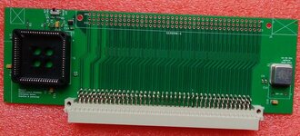
PDS_PGA.jpg
PGA socket instead of PLCC, and the oscillator moved from the right to under the '882. Other than that, same principle.

Works fine at 20 & 40 MHz in my IIsi. Performance improvement is measurable at 40 MHz, but not anywhere near x2 - IIRC, I had made the same observation running PovRay on the 3/80 back in the day. I guess a lot of time is spent doing bus transaction between the '030 and '882.

I probably should solder another one to put a '881 in, and finally do some '881 vs '882 measurement :) But those 188 solder points (plus 4 for the clock if installed) are a chore :-( I probably should do another PLCC as well with a 32 MHz clock to double-check if it's not the specific board itself that prevent the PLCC version to run at 32 MHz.

For those interested, both variants are on the GitHub.
 

Melkhior

Well-known member
Another attempt, another weirdness...

After fixing (sort of) some power stability issue in the IIsi and soldering the second DIN connector, the 32 MHz variant of the PLCC still doesn't work on its own, generating error 11 at 32 MHz. However, it was able to execute Spedometer 4.02 FPU benchmark at 32 MHz just fine when a PDS device I'm working on was plugged into the second connector! I'm guessing some issue with signal integrity? The design is not that different from the PGA version that works at 40 MHz stand-alone...
 

zigzagjoe

Well-known member
That is weird... It seems like error 11 is kind of a catch-all, I feel like if you knew what vector(s) trigger an 11 that'd help give some indication of what to troubleshoot. It might be interesting to figure out if it's any floating point instruction that does it (ie. FPU not responsive/insane) or a series of them that causes the error too. Do you have Macsbug installed?

Otherwise, if you can confirm the presence of the PDS card seems to help the problem, there's always the pull up/pull down assorted control signals that go to the 68882 and see what happens. None of them (used by the 68882) really jump out at me as likely to be immediately problematic, but it's easy enough to test with the second PDS socket.
 

ymk

Well-known member
However, it was able to execute Spedometer 4.02 FPU benchmark at 32 MHz just fine when a PDS device I'm working on was plugged into the second connector! I'm guessing some issue with signal integrity?

Very possible. Signals bounce back from traces that go nowhere.

You might see an improvement if the FPU lines meet the bus at the female connector, though it's not the shortest path.
 

Melkhior

Well-known member
It might be interesting to figure out if it's any floating point instruction that does it (ie. FPU not responsive/insane) or a series of them that causes the error too. Do you have Macsbug installed?

The '882 is detected by e.g. Speedo 4.02 or Tattletech, which I assume means something is sort-of working. I should try again with macsbug to see if the crash is deterministic or not.

Otherwise, if you can confirm the presence of the PDS card seems to help the problem (...)

I tried again, and Speed 4.02 could do multiple iterations of all FPU benchmarks with no issue with the PDS card installed. It never worked (instantaneous crash) without. So it definitely helps, even if I didn't test enough to say 'it works'.

I should try your suggestion of pull-up/down, as indeed with the female DIN installed it should be easy to add some THT resistor(s). The data lines are less likely to cause crashing issue (I don't know if Speed 4.02 checks the results, so it might be computing wrong! but that's the next step...), which leave /DSACK[01], /AS, /DS, /FPU, /RW and the four address lines as primary candidates. Still quite a few to try, in particular if more than one is causing issue. The local 32 MHz clock is unchanged by the presence of the PDS device, and /RESET shouldn't be involved once the machine is running, so those are out.

You might see an improvement if the FPU lines meet the bus at the female connector, though it's not the shortest path.

On the PLCC version the four address lines and the CPU clock are routed from the FPU to the top connector (along with /RESET). Everything else is routed to the bottom (motherboard-side) connector. On the PGA version (which work stand-alone at 40 MHz, did not solder a top connector yet), only the CPU clock and /RESET are connected to the top connector.

I did wonder if routing everything from the bottom connector would be better; it creates shorter paths to the FPU (hence my lutimate choice) but also a branch for every signals. Connecting to the top connector is as you said longer, but without the branch - is that the reason why you suggest it might be a better arrangement, or is it something else?
 

ymk

Well-known member
Connecting to the top connector is as you said longer, but without the branch - is that the reason why you suggest it might be a better arrangement, or is it something else?

That's the reason; it gets rid of the branch.

The same principles behind SCSI termination apply and the problems get worse with speed.

A branched, unterminated 3.3V clock signal on one of my projects measured >6V peak to peak due to reflections. 82 Ohm resistors to ground at each destination solved the problem, but that's not something you can do on the 030 bus.

Also, your logic analyzer has some capacitance, which may be enough to make or break operation.

 
Top