• Updated 2023-07-12: Hello, Guest! Welcome back, and be sure to check out this follow-up post about our outage a week or so ago.

Reverse Engineering the Macintosh IIsi Logic Board

Trash80toHP_Mini

NIGHT STALKER
Quick question about this one. Are layer count, complexity or board size problematic?

If not, the board seems like it might be worth doing in its original form and factor. But to me it seems to be a far more flexible platform for spinning off upgraded derivatives than anything else in the Macintosh II series, SE/30 included.

Given the amazing progress @Bolle has made and is now working on with his co-conspirators on the VidCard front, it may be time to take a look at possibilities?

Don't recall offhand, but if PPC upgrade capable, mashing a much enhanced version of the IIsi into the SE/30 form factor might lead to the SE/30/PPC of myth and impossible dreams?

Upgrade to a pair of 72pin SIMMs looks the plan as the hardware is limited on the board, ROM limit to less than 128MB seems unlikely?
Vampire Video subsystem removal frees up $E for far more capable video on board.
Multiple PDS expansion (NuBus Inclusive makes it more expandable at system clock and equals overall IIci expansion at four interrupts.
Three available I/O channels on PDS at 20MHz (or more) trumps the IIfx' NuBus I/O at 10MHz

Dunno, seems like the time to bounce this morning's musings off the wall? 🤪
 

max1zzz

Well-known member
So I actually acquired one of these a while back with the intention of reverse engineering it, However it is a 6 layer board so the "trace it in Sprint" method that @Kai Robinson and me have used before would not work for this one so this would need to more advanced "reverse a schematic first then redraw the board" that @Bolle used for the SE/30

This is actually kind of a good thing if you want to make changes to the board as modifying a board in sprint is truly headache inducing as it doesn't define connection nets!

At the moment this is not something I have any experience with but I plan to eventually get around to learning to do it (I'm currently getting my eye in by drawing schematics for the LC I (And probably also the Plus, LCII and LC III after that) and after that I have the LC 475 / Q605 board to do which also appears to be a 6 layer one)

However, If anyone wants to have a crack at reverse engineering the board now I am more than happy to pass to board I obtained on to someone else :)
 

Trash80toHP_Mini

NIGHT STALKER
That's music to my ears @max1zzz :D One of my several DOA boards is headed back to work with me after lunch!

I'll see about converting PCB pics, schematic and the bits I wish to retain from the block diagram into a rat's nest layered up in Illustrator. I'll need to ransack my files for the SIMMspender conversion of Bank A memory to 72pin SIMM sans Video Buffer complications.

One question, do you think POST verifies the video subsystem before or after it detects sense codes on the connector? Hope here is that DECLROM for substitute video at $E will get around that roadblock?

Definitely needs to be a socketed processor per BolleWerke developments. Haven't been obsessed with an impossible dream that I can chip away at myself in several years. 🤪
 
Last edited:

Trash80toHP_Mini

NIGHT STALKER
Found a bunch of my files this evening and also found the 601upgrade thread:


Melkhior

Well-known member
I'll see about converting PCB pics, schematic and the bits I wish to retain from the block diagram into a rat's nest layered up in Illustrator
Rather than a pure drawing program like Illustrator, might be worthwhile to redraw the schematics (e.g. from Bomarc) into a commonly available specialized piece of software like KiCad. Some of the components are already available as KiCad symbols from third-parties (e.g. the 68030 and 68882 are in Garrett's Workshop parts libraries, along with many others). That would make it a lot easier to subsequently recreate the original board (or even create "alternative" boards).
Also probably quite a bit of schematics are common between systems (some of the common I/O probably didn't change much between models, ditto power circuit) so there could be some work-sharing there. Is any II-class system already available in KiCad ?
 

Trash80toHP_Mini

NIGHT STALKER
Rather than a pure drawing program like Illustrator, might be worthwhile to redraw the schematics (e.g. from Bomarc) into a commonly available specialized piece of software like KiCad.
Old dog/new tricks/learning curves. ;) I've far better tools at hand than when developing the Rubyliths required for photographic PCB production process I did in the late eighties.

Visual thinker here, I can't "see" schematics at all. However ratlined PCB layouts all look like wire wrap boards to me. No problem there, stringing it together in Illustrator by connecting the dots of parts I've already done in that format will be a breeze.

I can easily tease the available IIsi Schematic***** apart into a functional version of the Block Diagram (Schematic's pages) of those two sources into neat and clean wire wrap design language. Modeling such in the PCB format will be within the scope of what I've already done using the talents I do have. No learning curve there.

At some point another member will be able to translate schematic and my graphics into a clean representation of same in KiCAD. That learning hurdle is for another day and simple projects I've back burnered over the years, expansion card risers, adapters and such.
 
Last edited:

Trash80toHP_Mini

NIGHT STALKER
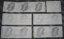
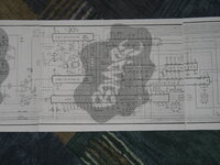
***** I bought the schematic from BOMARC years back, scanning, tweaking, printing and then cutting and taping it together into blocks I can see:

BOMARC-IIsi-Schematic_Assembly-00.JPG

Memory controller, banks A&B along with Vampire Video buffering are already assembled in the visual cortex and set up in layers of AI files. ;)
 
Last edited:

Melkhior

Well-known member
@Trash80toHP_Mini The Bomarc schematics are my point in a way; they already exist to offer a purely 'visual' view. It might be better to have a 'nicer' view in a modern program, but it would be even better to add some semantic to the drawings by using a schematic-oriented tool. I'm not sure an Illustrator drawing can be easily imported in of those...
OTOH, the volunteer doing the work is the one deciding which work the volunteer is going to do :)
 

Trash80toHP_Mini

NIGHT STALKER
Yep, enlisting the help of practioners of the black arts here is what I've done. Cranked up LEM's abandoned SE/30 PowerCache adapter project in the ProtoCache hacks thread series here and there with my doodles. Sorcerers @Bolle and @joethezombie picked up that ball and far outran anything I could ever do.

The BOMARC schematic is only visual to a point for me, setting up its models in AI diagrams of the components brings it into focus.
 
Last edited:

Trash80toHP_Mini

NIGHT STALKER
I'm thinking in terms of setting up my IIsi "layout" to fit the form factor of the SE/30. That'll be helpful to me by cutting corners overall and schematically thinking contributors won't "see" the difference anyway. Damn the legs, full speed to the hypotenuse. ;)
 

Trash80toHP_Mini

NIGHT STALKER
I could use (read: emphatically need) the help of a whiz at board rework with the recap of one of my several IIsi boards. I don't need it back, peeling away the layers of the monstrosity that is the Vampire Video buffered Bank A of the IIsi would be the challenge.

Uniserver upgraded a board to 4MB on those pads, so that's a start.

1) will the IIsi boot from Bank B in no sense lines detected state with Bank A depopulated?
2) if so, will the IIsi boot with Vampire Video buffering components excised?
3) if so, will the IIsi boot with the rest of the Video Subsystem components excised?

@max1zzz whatcha think?
 

Bolle

Well-known member
Looking at the IIsi and IIci schematics a little bit closer I start to wonder what's up with the PALs around the ASC on the IIsi?
The IIci uses the same MDU/RBV chipset combination and everything but doesn't have them...
 

Trash80toHP_Mini

NIGHT STALKER
OOPS! Was running out the door to work and mistook ASC for RBV, so it's not video.

IIsi has ASC from legacy Macintosh II architecture AND a an audio input jack that's lacking in the IIci.
Sound interface
The sound interface on the Macintosh IIsi computer has been
enhanced to include not only stereo sound output but also monaural
sound input. A microphone and RCA adaptor plug are shipped with
the Macintosh IIsi computer to facilitate the use of the sound input
feature.
Sound output
The sound output circuitry provides sound and four-voice synthesis
compatible with the Macintosh II family. It consists of the Apple
Sound Chip (ASC) and two Sony sound chips to filter the pulsewidth-
modulated signal and drive the on-board speaker or external
stereo microphone jack, as was done on the Macintosh II, Macintosh
IIx, Macintosh IIcx, and Macintosh IIci computers.
Sound input
The sound input circuitry consists of an input jack, an audio
filter/preamplifier, a FIFO buffer memory to store the digitized data,
and control logic to allow software to control the circuitry.
The main advantage of the Macintosh IIsi computer’s built-in sound
input over external sound input solutions is that the Macintosh IIsi
sound circuit is interrupt driven and is buffered by a large FIFO
buffer memory; therefore, less of the computer’s bandwidth is
required for sound input.

WAG here would be that those PALs are a Butt Ugly Bodge to force ASC into going both ways?

LCII DevNote looks to be a parallel development of sound subsystems unhindered by and leapfrogging legacy ASC architectural baggage? Has anyone ever found the mythical LC DevNote?

If that guess is correct, dunno if Kluge or BUB would be the proper qualifier for such a thing?

@max1zzz what's your read on sound I/O development in the 16bit versions of the LC series from scratch(?) to the LCIII's Sonora Integrated Controller and then onto the road to Prime Time ASIC of LC475/Q605?

I just took my very first peek at that architecture. :oops:

Quadra Archictecture stepped off the Macintosh II ASC path and onto the ECSC ASIC:

Sound ICs: DFAC, Enhanced ASC, and Sporty
The Macintosh Quadra 700 computer uses a new sound system. Its
features are similar to the features of the sound interface in the
Macintosh LC and the Macintosh IIsi. The features of the Macintosh
Quadra 700 sound interface include
· the ability to record monophonic sound from the microphone
input
· the ability to play 8-bit sound files
Three Apple custom ICs plus a digital-to-analog converter provide
the sound interface
· DFAC, which provides sound input and an antialiasing filter
· Enhanced ASC, an updated version of the Apple Sound Chip
· Sporty, a custom IC that replaces the two Sony sound ICs
· External digital-to-analog converter (DAC)
The DFAC (Digitally Filtered Audio Chip) is an Apple custom IC that
is also used in the Macintosh LC. The DFAC IC includes the
antialiasing filter and analog-to-digital converter (ADC) for sound
input.
For sound output, the Sporty custom IC replaces the two Sony ICs
used in earlier models and, together with the external DAC, provides
better sound quality with less noise and distortion. Like the Sony ICs
it replaces, the Sporty IC contains digital attenuators and power
amplifiers.
 
Last edited:

mmu_man

Well-known member
Starting from the schematics allows generating a proper netlist and in turn using them to make sure tracks are correct.
Also, while KiCAD started to standardize parts layout for schematics, and the usual placement is to have components as vertical blocs, it's quite possible to recompose and stretch them to reproduce the Bomarc design quite closely. Not sure it's desirable though.
And it's still possible to start putting traces in parallel while doing the schematics, and reconcile with the netlist later. Hackaday mentions a way to do it similarly to Sprint.
And KiCAD just got to version 6.0.
 

max1zzz

Well-known member
@max1zzz what's your read on sound I/O development in the 16bit versions of the LC series from scratch(?) to the LCIII's Sonora Integrated Controller and then onto the road to Prime Time ASIC of LC475/Q605?
I'm not a expert on the low down architecture of them, but my assumption would be that the sound capabilities of the LC I - III are more or less the same given they use the same external componentry (DFAC and similar amp stages), As for the later macs, I have no idea really as I haven't yet had any kind of in depth look at how the LC475 / Q605 work yet
 

Trash80toHP_Mini

NIGHT STALKER
GAH! :rolleyes: Just pulled my head out of the audio subsystem rabbit hole. Never mind LC development, that's a blind alley and unrelated to the Macintosh II series.

Interested to see what you've noodled out about those extra ASICs in the IIsi schematic @Bolle I got nothin' more and what I have got is likely wrong.

@mmu_man I think I hurt the part of my brain that does long division bulling my thru that Hackaday article. I think I'll stick with making pretty pictures in AI thank you very much. ;)
 
Last edited:

Trash80toHP_Mini

NIGHT STALKER
Gotta consult my conscience about that, never knew one was missing or wouldn't have posted the pic of it upthread. The mail ordered orange papers had an NDA/License attached. Not sure it's run out or has become moot since the uniserver leak? Scanner's down and out with the QS'02 graphics workstation at the moment anyway. :oops:

Looking into lopping that section off the available page above anyway. Excising audio input from the schematic seems the thing to do for the moment.

Speaking of which, has anyone booted a IIci from the IIsi ROM? Does the IIci crash and burn when Audio In hardware test fails to pass muster at POST?

I've got a bunch of boards and ROMS from testing from @dougg3 ROM SIMM development. ISTR the IIsi in a crumpled, smoking heap of wreckage with the IIci ROMs on board. If Audio In proves problematic, one ROM or the other may need a bit of hacking to boot this kluge up.
 
Last edited:
Top