• Updated 2023-07-12: Hello, Guest! Welcome back, and be sure to check out this follow-up post about our outage a week or so ago.

Early Macintosh home brew 4MB memory upgrade board development

Builder68

Active member
Agreed, that’s a great sign that it should work for this project!

Thanks for sharing this. I saw a blurb in the schematic in the linked GitHub repository talking about using an AND gate to control the ~OE line to the RAM ICs based on either the upper or lower ~CAS lines being asserted rather than just tying ~OE low like I had originally. The purpose for this allowing the use of EDO type RAM if FPM type becomes unavailable.

One more criterion to add to the list for the schematic redraw!
Good Catch! Linking that schematic was worth it!

I have to say, I find the way you use chat very enjoyable, like a kind of log of the thoughts, reflections, and decisions you make for the development of your project; it's much better than the stickers on the corkboard, isn't it? 😁
 

Golden Potato

Active member
Good Catch! Linking that schematic was worth it!

I have to say, I find the way you use chat very enjoyable, like a kind of log of the thoughts, reflections, and decisions you make for the development of your project; it's much better than the stickers on the corkboard, isn't it? 😁
Thanks! It can be a little meandering at time, but I find talking (or typing) my thoughts out loud helps me understand them better. Hopefully, it helps others too.
 

Golden Potato

Active member
I'm working on the schematic redraw, and I have an idea for connecting the ~OE pins on the DRAM ICs like the Mac Classic RAM expansion card without adding any new ICs. I'd like to hear opinions from others as the approach splits memory across the two DRAM ICs in a funny way.

The Mac Classic RAM expansion card Builder68 linked in a previous reply uses an AND gate on the two ~CAS lines (upper and lower bytes) for each DRAM, and the output of the AND gate is used to control the ~OE pins on each DRAM. To summarize the function: For each DRAM IC, if either the upper or lower ~CAS line is asserted, the ~OE pin is asserted on the IC. Only the corresponding upper or lower byte will actually output data. Apparently, this allows for EDO style DRAM ICs to be used in place of FPM.

1714933405238.png

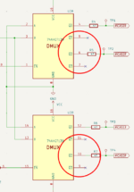
On my schematic, ~MCAS0F and ~MCAS1F could be connected to an AND gate to feed the ~OE pin for the DRAM IC which will receive those two ~CAS lines. The same could be done for ~MCAS2F and ~MCAS3F to the other DRAM IC. Scroll to the bottom of this reply to see it drawn on a schematic.

1714933746577.png

After some further thought, it occurred to me that in this design those four ~MCAS#F are derived from the 512K system's ~CAS0 and ~CAS1 lines. If the purpose of the AND gate is to combine two of the ~MCAS#F lines, why not skip it and drive the ~OE pins on the DRAM ICs with the 512K system's ~CAS0 and ~CAS1 for each of the two DRAM ICs directly? The downside to this is I wouldn't be able to take ~MCAS0F & ~MCAS1F to one DRAM IC and ~MCAS2F & MCAS3F to the other DRAM IC.

Take a look at the truth table for the 74LS138 which generates the ~MCAS#F signals. When ~CAS0 is asserted, either ~MCAS0F or ~MCAS2F will be asserted depending on the state of A21 or if the video hardware is accessing memory. Similarly, ~CAS1 drives either ~MCAS1F or ~MCAS3F. Thus, to drive the ~OE line for a DRAM IC from ~CAS0, that DRAM IC should be receiving ~MCAS0F and ~MCAS2F.
1714943664003.png

This means the DRAM IC containing the lower byte of the first 2MB of memory will also contain the lower byte for the second 2MB of memory. The other DRAM IC will contain the upper bytes for both the first and second 2MBs of memory. To summarize, instead of one 2MB 16-bit DRAM IC containing the first 2MB of memory (both upper and lower bytes) and another IC containing the second 2MB, one DRAM IC contains the lower bytes for all 4MB and the other IC contains the upper bytes for all 4MB. This doesn't seem so bad, except that it almost defeats the purpose for 16-bit DRAM ICs. Fortunately, the Mac 512K's RAM hardware only accesses one byte at a time, meaning either an upper or a lower byte, and never all 16-bits at once.

This is what it would look like:
1714950225938.png

Compare that to how I would have expected or wanted the schematic to be:
1714950543242.png

It seems like a minor difference, and I think either way would work just fine. Does saving one IC (and more propagation delay) justify complicating the schematic? The method without the AND gate would certainly make troubleshooting a faulty DRAM IC difficult since either IC is responsible for the entire 4MB memory (upper or lower bytes, of course). Granted there are only two DRAM ICs, so it's a 50/50 shot at which one could be the hypothetical problem.
 

Golden Potato

Active member
My mind wandered back to this project while I was at work today, and I couldn't help but think about how the technique I'm borrowing from "Classic Mac Tech Docs v1.1" to generate additional ~CAS lines only allows for upper or lower byte of RAM to be accessed at one time. That didn't sit right with me. There's no way the classic Macs are limited to only accessing upper or lower bytes at a time, and I'm unaware of any tricks going on such as data for each byte held in latches to present both bytes at once.

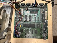
To confirm my suspicion, I reconnected my Mac 512K to stock configuration and probed the CAS0 and CAS1 lines, which correspond to lower and upper bytes of RAM, and found that the Mac does indeed access both banks at once for a full 16-bit word. Although sometimes only the upper or lower bytes are accessed.

Stock 512K CH1=CAS0 CH2=CAS1 LL.png

Stock 512K CH1=CAS0 CH2=CAS1 LH.png

Stock 512K CH1=CAS0 CH2=CAS1 HL.png

I haven't personally laid eyes on a Mac with the 1MB memory mod as described in that document, but I would be willing to bet that there isn't such a Mac in existence since it wouldn't work! The truth table for the 74LS138 (see previous reply) indicates that both CAS0 and CAS1 asserted (logic 0s) would select either output Y0 or Y1, depending on the state of A19 (A21 in my case), and both of those outputs are not connected to anything. Any 16-bit word accesses to RAM would not select any memory.

I wouldn't post this here without a solution in mind; adding a quad AND gate IC and making connections to those first two unused outputs on the 74LS138 takes care of cases where both ~CAS0 & ~CAS1 or ~CAS2 & ~CAS3 need asserted at once.

1715231792181.png

I'm really counting on the new DRAM's faster speed making up for any added propagation delay from the logic ICs here.

For my previous reply: I've decided to just go ahead and add the AND gates for EDO DRAM compatibility since I'm already adding another IC here. I'd prefer a readable schematic over some tricks to save one small IC since this is just a hobby project.
 
Last edited:
Top